
Back to blog
PCB Flying Probe Test: What Is It? How It Works?

What is PCB Flying Probe Test
The PCB Flying Probe Test is an advanced method used in the electronics manufacturing industry for testing the electrical functionality of Printed Circuit Boards (PCBs). Named for its distinctive use of movable probes that ‘fly’ over the PCB to make contact with various points, this test is a cornerstone in ensuring the quality and reliability of PCBs.
Flying probe testing is most effective when the design leaves reachable nets and clear test intent, so it should be planned with PCB electrical testing requirements and, for functional coverage, a suitable PCBA test strategy.
Unlike traditional testing methods that use fixed test fixtures (like the bed of nails), the flying probe test utilizes a number of robotic arms equipped with precise probes. These probes are programmed to move to specific points on the PCB to conduct tests.
The Significance in PCB Manufacturing
- Detecting Manufacturing Defects: The primary purpose of the flying probe test is to identify manufacturing defects such as open circuits, short circuits, and component issues. It’s particularly effective for complex PCBs where traditional testing methods may fall short.
- Versatility and Flexibility: This method is highly adaptable to different PCB designs without the need for custom fixtures. It can be reprogrammed for different PCB layouts, making it ideal for prototyping and small to medium production runs.
- Non-Destructive Testing: The flying probe test is a non-destructive method, meaning it tests the PCB without causing any damage. This is crucial for maintaining the integrity of the board, especially in delicate or high-value applications.
How Does the PCB Flying Probe Test Work?
Step 1: Setup and Programming
Initially, the specific PCB design is loaded into the test software. This includes the PCB layout and the electrical characteristics expected at each test point.
The software then creates a testing sequence, programming the movements of the probes to align with the layout of the PCB.
Step 2: Contact and Measurement
During testing, the probes gently touch the test points on the PCB. The test points can include component pads, vias, or any other conductive part of the PCB.
The probes measure various electrical properties, such as continuity, resistance, capacitance, and sometimes more complex parameters like frequency response or logic functionality.
Step 3: Analysis and Reporting
After data collection, the system analyzes the results by comparing them to the expected outcomes defined in the PCB design specifications.
Any discrepancies or anomalies detected are flagged. This could indicate potential issues such as short circuits, open circuits, or defective components.
Flying Probe Test VS Traditional Methods
Traditional PCB testing often involves methods like the ‘Bed of Nails’ tester. This system uses a custom fixture with numerous pins (nails) that align with test points on the PCB. When the PCB is pressed against these pins, electrical tests are conducted across the board.
Flexibility and Setup Time
Flying Probe Test: Offers exceptional flexibility, as it doesn’t require custom fixtures. The setup time is significantly reduced, as the test programming is based on the PCB design files. This makes it ideal for prototypes and small production runs where design changes are frequent.
Traditional Methods: The setup involves creating a custom fixture, which can be time-consuming and costly. This method is more suitable for large-scale production where the design is finalized and unchanged over many units.
Cost Implications
Flying Probe Test: While the initial cost of a flying probe tester can be high, it eliminates the need for custom test fixtures, making it more cost-effective for low-volume or varied productions.
Traditional Methods: Require a significant upfront investment in custom fixtures. However, for high-volume production, this cost is amortized over many units, potentially making it more economical in the long run.
Testing Capabilities
Flying Probe Test: Capable of performing detailed and precise tests. It can easily adapt to test different PCBs, making it versatile for testing complex or densely packed boards.
Traditional Methods: While effective for general testing, they may not match the precision of flying probe testers, especially for highly dense or complex PCBs.
Speed and Throughput
Flying Probe Test: Generally slower than traditional methods due to the time taken for probes to move and test different points. Best suited for situations where testing speed is less critical than flexibility.
Traditional Methods: Offer faster testing per PCB, making them more efficient for high-volume production where the same design is tested repeatedly.
Quality and Reliability
Flying Probe Test: Provides high-quality testing with detailed analysis. Its ability to quickly adapt to design changes ensures thorough testing for each unique PCB.
Traditional Methods: Reliable for consistent testing of uniform PCBs. However, they may not be as effective in detecting certain types of defects on complex or non-standard boards.

Related Articles
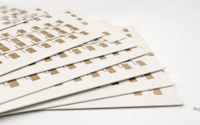
Rogers TMM Antenna PCB Manufacturing for Patch, Array and mmWave Designs
Detailed Rogers TMM antenna PCB guide for patch antennas, arrays, mmWave, Dk selection, bandwidth, feed networks, fabrication controls and quote checklist.
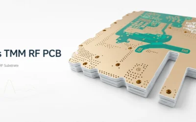
Rogers TMM RF PCB Design and Manufacturing for Controlled Impedance
Detailed Rogers TMM RF PCB guide for controlled impedance, 50 ohm traces, microstrip, GCPW, stripline, RF loss, surface finish, layout and quotation.
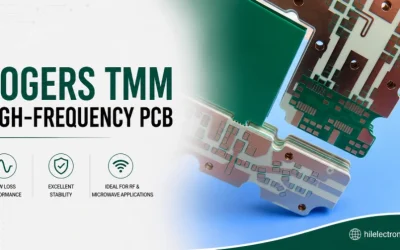
Rogers TMM High-Frequency PCB Manufacturing
Rogers TMM high-frequency PCB guide covering TMM3–TMM13i Dk/Df, grade selection, stackup, impedance, copper, fabrication, comparison and RF quote checklist.