
PCB Measling Prevention and Delamination Control

Printed Circuit Boards (PCBs) are at the heart of modern electronic devices, and their reliability is critical to the proper functioning of complex systems. Two major defects that can undermine the integrity of a PCB are measling and delamination. Both are forms of laminate degradation, but they differ in severity and causes. Understanding and preventing these issues is crucial for ensuring long-term durability and reliability of PCBs, particularly in high-stress environments such as aerospace, automotive, and medical industries.
What is PCB Measling?
Measling refers to the appearance of white spots or “measles” within the fiberglass-reinforced laminate of a PCB. These spots are typically small, localized areas of delamination within the resin matrix, where the glass fibers have separated from the resin, creating voids. While measling does not usually cause immediate electrical failure, it weakens the laminate structure and can potentially lead to more serious issues such as delamination if the board is subjected to further stress.
Causes of Measling
Measling occurs due to a combination of thermal and mechanical stress. Common causes include:
-
Thermal Shock: During soldering or other high-heat processes, rapid temperature changes can cause the resin to contract more rapidly than the glass fibers, leading to separation and the formation of measles.
-
Moisture Absorption: Fiberglass is inherently hygroscopic, meaning it can absorb moisture from the environment. When the PCB is exposed to high temperatures, this moisture turns to vapor, creating pressure within the laminate that forces the fibers to separate from the resin.
-
Poor Lamination: Inadequate lamination techniques during PCB manufacturing, such as insufficient pressure or improper curing, can leave gaps or air pockets within the laminate. These gaps can expand under stress, leading to the development of measles.
Impact of Measling on PCB Performance
While measling is primarily a cosmetic defect at first, it indicates a weakening of the laminate structure. If left unaddressed, measling can escalate into larger delamination problems, particularly in high-stress applications. In critical sectors such as aerospace or military electronics, where reliability is paramount, even minor cases of measling can lead to rejection during quality control checks, as these white spots are often seen as precursors to more severe degradation.
Delamination of PCBs
Delamination refers to the separation of layers within the PCB laminate. It is a more severe issue compared to measling and can cause immediate and catastrophic electrical failure. Delamination occurs when the bond between the copper layers and the dielectric (usually FR4 or polyimide) or between layers of dielectric material themselves breaks down. This separation can cause open circuits, shorts, or the complete disconnection of signal paths.
This page is the prevention guide for measling and delamination. If a board already shows symptoms, use measling and delamination failure analysis; for inspection records and repeat-order controls, review Highleap’s PCB quality assurance process.
Common Causes of PCB Delamination
Several factors contribute to delamination of PCBs, including:
- Thermal Cycling: Repeated exposure to high and low temperatures causes the materials within the PCB to expand and contract at different rates. If the thermal coefficient of expansion (TCE) between the copper and the dielectric material is mismatched, the resulting stress can lead to the separation of layers.
- Moisture Entrapment: During the PCB manufacturing process, moisture can get trapped in the laminate. When the board is exposed to high heat during soldering or reflow, this moisture vaporizes and expands, causing blistering and layer separation.
- Improper Lamination Process: Poor lamination techniques, such as inadequate heat, pressure, or curing time, can lead to weak bonding between layers. Voids, air pockets, and uneven adhesion can eventually lead to delamination under stress.
- Chemical Exposure: PCBs used in industrial environments or exposed to harsh chemicals during manufacturing are at risk of chemical degradation of the adhesive materials. This degradation weakens the bond between the copper and dielectric, leading to layer separation over time.
Effects of PCB Delamination
The effects of delamination are often immediate and catastrophic. Once delamination occurs, the structural integrity of the board is compromised, leading to several critical issues:
- Open Circuits: Delamination can cause the copper traces to disconnect from the dielectric, resulting in open circuits that prevent the board from functioning properly.
- Short Circuits: In multilayer PCBs, delamination can cause different layers of copper to come into contact, leading to short circuits and potential damage to connected components.
- Increased Resistance and Signal Degradation: Even if complete separation has not occurred, partial delamination can increase resistance in the signal paths, leading to signal degradation, loss of signal integrity, and overall poor performance.
For a more complete production review, use this article alongside LED aluminum PCB production and Rogers PCB manufacturing when checking stackup, assembly, or test requirements.
Delamination vs. Measling
While measling and delamination are both forms of PCB laminate failure, they differ significantly in terms of their severity, causes, and effects:
- Measling is a more subtle, early-stage issue, often appearing as small white spots in the fiberglass bundles. It indicates weakness within the laminate but does not immediately cause electrical failures. However, if left unaddressed, measling can eventually lead to delamination.
- Delamination, on the other hand, is a severe structural failure in which layers of the PCB laminate separate. This can lead to immediate and catastrophic electrical failure, including open circuits and short circuits. Delamination requires immediate attention and repair, as it can compromise the entire functionality of the board.
Prevention of PCB Measling and Delamination
Both measling and delamination are preventable through careful material selection, manufacturing processes, and quality control. Some of the key strategies to prevent these issues include:
- Material Selection: Using high-quality laminates with appropriate thermal expansion coefficients can reduce the risk of delamination. Laminates with low moisture absorption rates are also crucial in preventing both measling and delamination.
- Proper Lamination Techniques: Ensuring the correct heat, pressure, and curing time during the lamination process is essential for creating strong bonds between the PCB layers. Adequate lamination pressure minimizes the risk of voids or air pockets, which can later expand and lead to delamination.
- Moisture Control: PCBs should be stored in low-humidity environments, and pre-baking the boards before soldering can help remove trapped moisture, reducing the risk of delamination during thermal cycling.
- Thermal Stress Management: Implementing effective thermal management solutions, such as thermal vias or heat sinks, can reduce the thermal stress on PCBs, minimizing the risk of both measling and delamination.
- Testing and Quality Control: Rigorous testing, including thermal cycling, humidity tests, and mechanical stress tests, should be part of the PCB manufacturing process to identify any potential weaknesses in the laminate before the board is assembled.
Conclusion
PCB measling and delamination represent serious challenges in PCB manufacturing and usage, particularly in high-reliability applications where even minor defects can lead to significant failures. Understanding the causes, effects, and prevention of these issues is essential for maintaining the long-term reliability of PCBs. By carefully managing materials, manufacturing processes, and testing procedures, manufacturers can minimize the risk of these defects and ensure that their PCBs perform reliably under demanding conditions.
For businesses looking to ensure the highest quality and reliability in their PCBs, working with experienced manufacturers who understand the intricacies of delamination of PCBs and how to prevent it is crucial. By investing in high-quality processes and materials, companies can avoid costly failures and ensure their electronic systems perform optimally for years to come.
Get a Free PCB & PCBA Quote

Recommended Posts
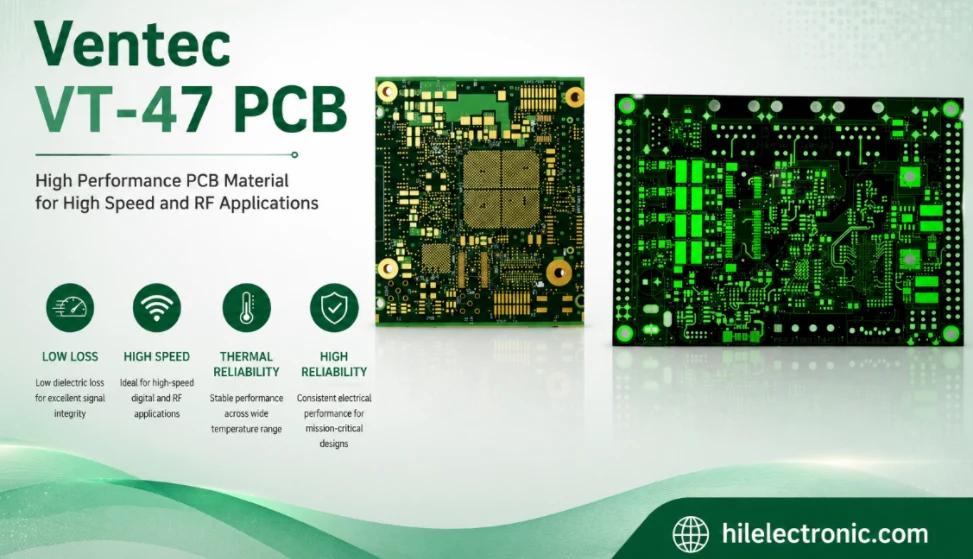
Ventec VT-47 PCB Manufacturer for Reliable High-Tg FR-4 Multilayers
Table of contentsIs Ventec VT-47 the Right High-Tg FR-4...
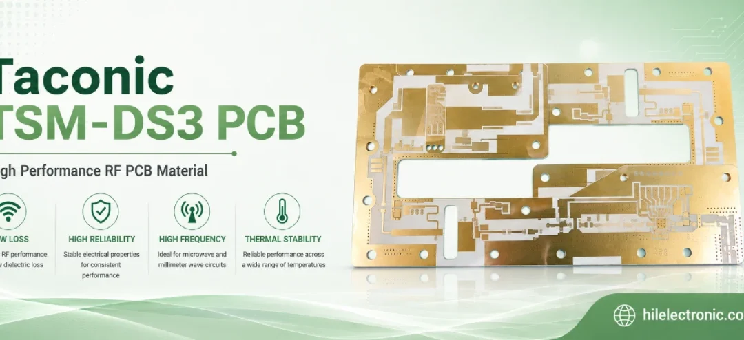
Taconic TSM-DS3 PCB Manufacturer for Thermally Stable RF Multilayers
Table of contentsWhen TSM-DS3 Is the Better RF...
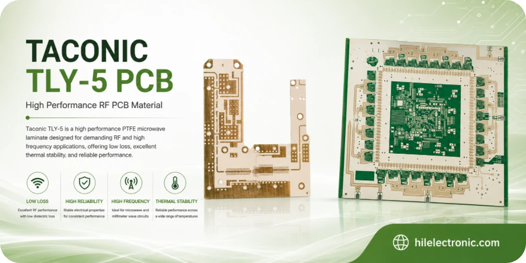
Taconic TLY-5 PCB Manufacturer for 77 GHz Radar and Antennas
Table of contentsCan TLY-5 Meet Your 77 GHz or Antenna...

RF Transceiver PCB Manufacturing and Assembly
Table of contentsRF Transceiver PCB Manufacturing and...
How to get a quote for PCBs
Let us run DFM/DFA analysis for you and get back to you with a report.
You can upload your files securely through our website.
We require the following information in order to give you a quote:
-
- Gerber, ODB++, or .pcb, spec.
- BOM list if you require assembly
- Quantity
- Turn time
In addition to PCB manufacturing, we offer a comprehensive range of electronic services, including PCB design, PCBA (Printed Circuit Board Assembly), and turnkey solutions. Whether you need help with prototyping, design verification, component sourcing, or mass production, we provide end-to-end support to ensure your project’s success. For PCBA services, please provide your BOM (Bill of Materials) and any specific assembly instructions. We also offer DFM/DFA analysis to optimize your designs for manufacturability and assembly, ensuring a smooth production process.