
Tips for PCB Wiring and Layout

Printed Circuit Board (PCB) wiring is the core element that enables electronic devices to perform their intended functions. Wiring a PCB involves the strategic layout and routing of conductive traces that interconnect electronic components, delivering signals and power. As electronic devices become more complex and demanding in terms of performance, designing effective PCB wiring requires deep technical knowledge and meticulous planning.
This article offers a comprehensive examination of PCB wiring, covering the basic principles of PCB layout and wiring, advanced routing strategies, manufacturing processes, materials considerations, and emerging trends in the field.
1. Basics of PCB Layout and Wiring
1.1 Fundamental Principles of PCB Layout
The layout of a PCB refers to the arrangement of electronic components and the paths of electrical connections between them. An optimal PCB layout is key to achieving the desired electrical performance, thermal management, and manufacturability. Several fundamental principles guide the layout process:
- Component Placement: Proper placement of components is crucial to minimize signal path lengths, reduce noise, and enhance thermal dissipation. Placing critical components like processors, memory, and power supplies first helps streamline the overall design.
- Power and Ground Plane Management: The inclusion of solid ground and power planes ensures a stable voltage reference for signals and reduces noise and electromagnetic interference (EMI). Proper design of these planes is essential for maintaining signal integrity.
- Partitioning and Segmentation: Separating analog, digital, and high-power sections of the PCB reduces interference and improves overall board performance.
1.2 PCB Wiring Fundamentals
PCB wiring, also known as routing, involves creating electrical pathways to connect components. Wiring is performed with specific considerations for trace widths, spacing, and routing techniques to meet electrical and mechanical requirements. Some basic principles include:
- Trace Width Calculation: Determined by the current-carrying capacity and allowable voltage drop. Wider traces are used for power lines, while narrower traces are common for low-current signals.
- Controlled Impedance: Necessary for high-speed signal traces to minimize reflections and signal degradation. Trace impedance is managed by adjusting trace width, distance from the reference plane, and the dielectric properties of the substrate.
- Via Types and Placement: Vias connect different layers of a PCB and include through-holes, blind vias, and microvias. The selection of via types depends on design complexity and signal integrity requirements.
2. Advanced Techniques in PCB Wiring
2.1 Differential Pair Routing
Differential pairs consist of two traces that carry equal and opposite signals, minimizing noise and improving signal integrity. High-speed interfaces, such as USB, HDMI, and Ethernet, use differential pairs. Key considerations for differential pair routing include:
- Length Matching: Differential pairs must have equal lengths to maintain timing synchronization and prevent skew. Uneven lengths can lead to differential-to-common-mode noise conversion, impacting performance.
- Controlled Spacing: Maintaining a consistent spacing between the traces of a differential pair is crucial to achieve the desired differential impedance. This spacing should be set based on the impedance requirements of the interface.
2.2 High-Density Interconnect (HDI) Techniques
As devices shrink and demand more layers and complex wiring, HDI techniques come into play. HDI PCBs use smaller vias, narrower traces, and advanced interconnect methods to accommodate higher component densities.
- Microvias and Laser Drilling: Microvias are small-diameter vias drilled using lasers, connecting adjacent layers. They allow designers to create finer wiring structures, enhancing the density and performance of the PCB.
- Stacked and Staggered Vias: Stacked vias align vertically across multiple layers, enabling direct interconnections through several layers. Staggered vias alternate in positioning, offering flexibility in routing.
2.3 Serpentine Routing and Length Matching
Serpentine routing introduces controlled delays in signal paths to maintain timing alignment between high-speed signals. This technique is particularly useful in data buses and parallel interfaces, where synchronized signal arrival is crucial.
- Calculating Signal Propagation Delays: Ensuring matched trace lengths requires precise calculations based on signal speed and board material properties.
- Serpentine Pattern Design: Designing the serpentine pattern involves creating a meandering path while maintaining minimal coupling between adjacent traces to avoid additional interference.

3. Signal Integrity and Power Integrity Considerations
3.1 Impedance Control for High-Speed Designs
In high-speed designs, maintaining controlled impedance is essential for preserving signal integrity. Controlled impedance is achieved by carefully adjusting trace width, thickness, distance from reference planes, and the substrate’s dielectric properties. Designers often use simulation tools and impedance calculators to optimize trace characteristics.
- Microstrip and Stripline Structures: Microstrip configurations have signal traces on the outer layer, while stripline configurations are embedded between ground planes. Stripline structures are preferred for reducing external noise interference but can increase manufacturing complexity.
3.2 Crosstalk and EMI Reduction
Crosstalk arises from capacitive and inductive coupling between adjacent traces, causing signal distortion. Minimizing crosstalk is crucial in dense designs and high-speed PCBs:
- Trace Spacing and Layer Separation: Increasing the distance between parallel traces and separating sensitive signals into different layers can significantly reduce capacitive coupling.
- Ground Guard Traces and Shielding: Placing ground traces adjacent to sensitive signals or using metal shields helps absorb interference and maintain signal integrity.
4. Materials and Manufacturing Techniques in PCB Wiring
4.1 Substrate and Dielectric Materials
The choice of substrate material impacts not only the mechanical properties of the PCB but also its electrical characteristics. Common materials and their properties include:
- FR-4: A widely used and cost-effective substrate material with a dielectric constant of around 4.5. Suitable for most general-purpose designs.
- High-Frequency Laminates (e.g., Rogers): These materials have lower dielectric constants (around 3.0) and low loss tangents, making them ideal for RF and microwave applications.
- Polyimide and PTFE-Based Laminates: Preferred for flexible circuits and high-temperature applications due to their superior thermal and electrical properties.
4.2 Advanced Plating and Surface Finishes
Copper plating and surface finishes are essential for ensuring good electrical connections and protecting the copper traces from oxidation. Different finishes offer trade-offs between cost, reliability, and solderability:
- Electroless Nickel Immersion Gold (ENIG): Provides a flat surface with excellent corrosion resistance and solderability, making it ideal for fine-pitch components and HDI designs.
- Organic Solderability Preservative (OSP): A cost-effective finish that protects copper but has a shorter shelf life compared to ENIG.
- Immersion Silver and Tin: Offer good solderability at a lower cost than ENIG but may require additional handling precautions to prevent tarnishing.
5. Manufacturing Techniques and Challenges in PCB Wiring
5.1 Photolithography and Etching for Fine Feature Sizes
Photolithography and etching are the primary methods for creating fine wiring patterns on a PCB. Advances in photolithography techniques, such as direct laser imaging (DLI), allow manufacturers to achieve finer line widths and smaller via sizes with greater precision.
Key Steps in Photolithography and Etching:
- Photoresist Application: A light-sensitive resist is applied to the copper surface.
- Exposure and Development: A photomask defines the desired wiring pattern, and UV light hardens the exposed resist.
- Etching: The unexposed areas are removed, and a chemical solution etches away the unwanted copper.
5.2 Mechanical vs. Laser Drilling for Vias
Vias are essential for establishing electrical connections between layers. Mechanical drilling is common for standard through-hole vias, while laser drilling is used for creating microvias and blind/buried vias in HDI designs. Laser drilling provides the precision required for advanced multilayer designs.
Considerations for Via Formation:
- Plating Reliability: The quality of via plating impacts the electrical connectivity and long-term reliability of the board. Ensuring uniform copper plating thickness is crucial, particularly for high-reliability applications.
- Via Filling and Capping: For stacked or sequentially laminated HDI designs, via filling and capping processes are used to reinforce the structure and create flat surfaces for component placement.
6. Thermal Management and Mechanical Integrity in PCB Wiring
6.1 Thermal Management Techniques
Proper thermal management is essential to maintain the reliability of high-power or densely populated PCBs. Techniques include:
- Thermal Vias and Heat Sinks: Thermal vias transfer heat away from critical components to heat sinks or metal cores. Heat sinks attached directly to high-power components help dissipate excess heat.
- Copper Thickness and Trace Width: The use of thicker copper (e.g., 2 oz/ft² or more) and wider traces in power sections helps reduce resistance and prevent thermal buildup.
6.2 Mechanical Considerations for Flexible and Rigid-Flex PCBs
Flexible and rigid-flex PCBs offer advantages in compact and dynamic applications but require careful mechanical design to avoid reliability issues:
- Stress Distribution and Bending Radius: Traces on flexible circuits should be routed with gradual bends and ample radii to minimize mechanical stress and prevent cracking.
- Layer Count and Stack-Up: Determining the optimal number of layers and stack-up configuration ensures adequate rigidity without compromising flexibility.
Conclusion
PCB wiring is a sophisticated and multi-faceted process that demands a strong understanding of design principles, material properties, and manufacturing techniques. This article has explored the basics of PCB layout and wiring, advanced techniques such as differential pair routing and HDI strategies, and considerations for signal integrity, thermal management, and mechanical robustness.
As electronic devices continue to evolve, PCB designers must remain informed about the latest trends and best practices. By mastering these techniques, engineers can create reliable, high-performance PCBs that meet the ever-growing demands of modern electronics.
Get a Free PCB & PCBA Quote

Recommended Posts
ITEQ IT-968G PCB for High-Speed Switch and Radar Designs
ITEQ IT-968G sits in the practical middle of the...
ITEQ IT-988GSE PCB for Ultra-Low-Loss 100G and 400G Backplanes
An IT-988GSE PCB should be selected from the channel loss...
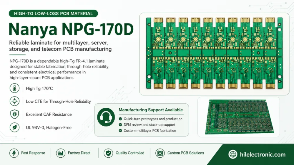
Nanya NPG-170D PCB Manufacturing for High-Tg Multilayers
Nanya NPG-170D PCB manufacturing should be planned as a...

Panasonic MEGTRON 7N PCB Manufacturing for High-Speed HDI
Panasonic MEGTRON 7N PCB manufacturing is a high-speed...
How to get a quote for PCBs
Let us run DFM/DFA analysis for you and get back to you with a report.
You can upload your files securely through our website.
We require the following information in order to give you a quote:
-
- Gerber, ODB++, or .pcb, spec.
- BOM list if you require assembly
- Quantity
- Turn time
In addition to PCB manufacturing, we offer a comprehensive range of electronic services, including PCB design, PCBA (Printed Circuit Board Assembly), and turnkey solutions. Whether you need help with prototyping, design verification, component sourcing, or mass production, we provide end-to-end support to ensure your project’s success. For PCBA services, please provide your BOM (Bill of Materials) and any specific assembly instructions. We also offer DFM/DFA analysis to optimize your designs for manufacturability and assembly, ensuring a smooth production process.