
Comprehensive Guide to PCB Circuit Board Design

PCB design is at the heart of modern electronics, driving innovation across consumer electronics, automotive, telecommunications, and more. The design of a PCB involves a detailed process that blends electrical, thermal, and mechanical considerations to deliver a reliable and high-performing product. In this article, we’ll explore the principles, techniques, and best practices for PCB circuit board design, focusing on achieving optimal electrical performance, manufacturability, and reliability.
1. The Fundamentals of PCB Design
1.1 Schematic Development and Design Intent
The initial stage of PCB design is schematic creation, which defines the electrical connections and functionality of the circuit. A well-structured schematic forms the basis for effective PCB layout and routing. Key steps in schematic development include:
- Component Selection: Choose components based on electrical specifications, thermal limits, and lifecycle availability. Prioritize components with well-documented characteristics to ensure stable supply and support.
- Power and Signal Distribution: Define the power distribution network (PDN) with appropriate decoupling capacitors and power regulation circuits. Organize signal flow logically to minimize potential cross-talk or interference.
1.2 PCB Layer Stack-Up Planning
Layer stack-up is a critical design aspect that influences signal integrity, thermal dissipation, and manufacturability. A balanced layer stack-up ensures robust signal routing, controlled impedance, and effective grounding. Best practices include:
- Even Layer Count: Maintaining an even number of layers prevents warping during manufacturing and provides balanced electrical characteristics.
- Ground and Power Plane Placement: Allocate solid ground and power planes adjacent to signal layers to provide reference points and reduce electromagnetic interference (EMI).
Our team specializes in designing optimized stack-ups tailored to the specific requirements of high-speed, high-power, and mixed-signal applications.
1.3 Component Placement for Optimal Performance
Component placement defines the layout strategy, impacting signal integrity, routing complexity, and thermal management. During placement, we focus on:
- Critical Signal Path Minimization: Place critical components such as clock oscillators, analog front-ends, and RF circuits in locations that minimize signal path lengths and noise exposure.
- Thermal Management: Distribute high-power components across the PCB to avoid creating localized hotspots. Utilize thermal vias and dedicated copper pours to enhance heat dissipation.
2. Techniques for Effective Routing
2.1 Differential Pairs and High-Speed Signal Routing
High-speed differential pairs are essential in designs involving USB, Ethernet, HDMI, and PCIe interfaces. To achieve optimal performance, we apply several key techniques:
- Length Matching: For differential pairs, we match trace lengths to within a fraction of a millimeter to avoid skew and ensure synchronous signal transmission.
- Controlled Impedance: Differential pairs require precise control of impedance, which is achieved by maintaining consistent trace widths and spacing. Our designs account for trace geometries and layer stack-up properties to meet target impedances (typically 90Ω to 100Ω for differential pairs).
2.2 Power Distribution and Decoupling
Ensuring stable power delivery is a fundamental requirement for all PCBs. We achieve this by implementing a well-structured power distribution network (PDN) with the following considerations:
- Dedicated Power and Ground Planes: Solid planes reduce voltage fluctuations and provide low-impedance paths for return currents. We allocate separate planes for critical power rails to prevent noise coupling.
- Decoupling Strategy: Decoupling capacitors are placed close to integrated circuits to filter high-frequency noise. We analyze and optimize capacitor values and placement using simulation tools to achieve the desired power integrity.
2.3 Mitigating Crosstalk and Electromagnetic Interference (EMI)
Crosstalk and EMI are common issues in dense, high-speed designs. Our approach includes:
- Trace Spacing and Guard Traces: We follow industry guidelines to maintain at least 3 times the trace width spacing between critical signals to minimize capacitive coupling. Guard traces connected to the ground plane are used to further isolate high-frequency signals.
- Layer Segmentation: Separating high-speed, noisy signals from low-frequency analog or digital signals reduces mutual interference and enhances overall signal integrity.
3. Advanced Signal Integrity and Power Integrity Considerations
3.1 Signal Integrity (SI) Analysis and Modeling
Signal integrity issues such as reflections, ringing, and attenuation can severely degrade PCB performance. We utilize advanced simulation tools, including HyperLynx and SiSoft, to model and address these issues. Our methods include:
- Impedance Control: Precise control of impedance in signal traces ensures minimal reflection and noise. We design with target impedance values based on the specific requirements of high-speed protocols.
- Minimizing Via Stubs: Via stubs can create impedance discontinuities. We apply techniques like back-drilling or use blind vias in multi-layer boards to eliminate stubs and improve signal quality.
3.2 Power Integrity (PI) and Grounding
Power integrity ensures stable voltage levels across the board. Our key techniques for achieving robust PI include:
- Power Plane Decoupling: Placing capacitors close to power pins and choosing appropriate capacitor types and values based on resonance frequencies.
- Ground Plane Stitching: We strategically place stitching vias between ground planes to provide a continuous low-impedance return path for high-frequency signals, minimizing ground bounce and noise.

4. Manufacturing and Testing Considerations
4.1 Design for Manufacturability (DFM)
A successful PCB design not only functions well but can also be manufactured reliably and cost-effectively. We integrate Design for Manufacturability (DFM) principles to streamline production:
- Trace and Via Tolerances: We follow IPC standards for minimum trace widths, clearances, and via dimensions to ensure compatibility with manufacturing capabilities.
- Thermal Reliefs and Soldering: Proper thermal reliefs are added to pads connected to large copper areas to improve soldering during the reflow process. This reduces the risk of cold joints and improves yield.
4.2 Design for Testing (DFT)
Ensuring the PCB can be efficiently tested is crucial for quality control. Our DFT strategies include:
- Test Point Placement: We provide dedicated test points for key signals, voltage rails, and communication lines. These test points facilitate easy access during functional and in-circuit testing (ICT).
- Boundary-Scan Implementation: For complex digital designs, we incorporate boundary-scan testing features to verify interconnects and component functionality without physical probing.
4.3 Thermal Management and Reliability
Thermal management is a critical aspect of PCB design, especially for high-power or densely populated boards. Our strategies include:
- Thermal Via Arrays: To dissipate heat from high-power components, we use dense thermal via arrays that transfer heat to the internal ground or power planes.
- Thermal Simulations: We perform thermal simulations to predict temperature profiles and identify hotspots. This helps us plan for additional cooling solutions like heat sinks, thermal pads, or airflow considerations.
5. Service Offerings for PCB Design
At our organization, we provide a comprehensive suite of services to support your PCB design needs from start to finish. Our services include:
- End-to-End PCB Design Solutions: We offer full-cycle design services, from schematic creation and component selection to layout, routing, and design validation.
- Signal Integrity and EMC Analysis: Our team specializes in signal integrity and EMC simulations to ensure that your designs meet performance and regulatory requirements.
- Prototyping and Manufacturing Support: We work with trusted fabrication partners to produce prototypes, enabling you to validate designs quickly and effectively.
- Design Optimization and Cost Reduction: We review and refine existing designs to reduce production costs, improve performance, and enhance reliability without compromising quality.
With our technical expertise and end-to-end services, we help clients navigate the complexities of PCB design, ensuring successful product development and deployment.
6. If You Need PCB Reverse Engineering Services
Reverse engineering of PCBs involves the process of reconstructing the design and understanding the functionality of an existing circuit board without having the original design files or schematics. This service is critical in scenarios where original documentation is lost, obsolete, or unavailable, and in cases where a detailed analysis of an existing product is required for improvement or replication.
Our expertise in PCB reverse engineering enables us to provide comprehensive support in recovering original designs, updating legacy systems, and enhancing existing designs. Here’s what our PCB reverse engineering services encompass:
6.1 Accurate PCB Design Reconstruction
One of the primary goals of reverse engineering is to recreate an accurate and detailed PCB design, including all the critical electrical, mechanical, and thermal characteristics of the original board. Our approach involves:
- High-Resolution Scanning: We utilize advanced high-resolution scanning equipment to capture all layers of the PCB, including internal traces, via placements, and component footprints. This scanning process helps to identify the exact layout and connections.
- Layer-by-Layer Analysis: By carefully analyzing each individual layer, we reconstruct multi-layer PCBs accurately. This includes identifying blind and buried vias, intricate routing, and complex ground and power planes.
- Schematic Generation: We create accurate schematics based on the analyzed PCB design, capturing the logical relationships and signal flow between components.
6.2 Component Identification and Bill of Materials (BOM) Creation
Reverse engineering a PCB requires detailed knowledge of component identification and sourcing. We focus on:
- Component Identification: We meticulously identify and verify each component on the PCB, including standard and custom parts, using techniques such as decapping for encapsulated components and pinout verification.
- BOM Generation: We generate a comprehensive Bill of Materials (BOM) that lists all components, specifications, and sourcing information. Where components are obsolete or unavailable, we recommend and validate suitable replacements.
6.3 Electrical and Signal Integrity Analysis
A critical aspect of PCB reverse engineering is ensuring that the reconstructed design performs identically to the original in terms of signal integrity, power delivery, and thermal characteristics. Our process includes:
- Electrical Circuit Testing: We perform functional tests on the existing PCB to understand its behavior and validate its electrical characteristics. This helps to confirm that the reconstructed design matches the original performance.
- Signal Integrity Assessment: During reverse engineering, we analyze the reconstructed PCB’s signal paths to ensure that impedance, crosstalk, and noise characteristics align with the original specifications.
6.4 Upgrading and Enhancing Legacy PCBs
Reverse engineering often presents opportunities to enhance or upgrade existing designs to meet modern standards or requirements. We offer:
- Component Upgrading: For legacy designs with outdated or obsolete components, we identify modern replacements that offer improved performance or availability.
- Design Optimization: We refine the reverse-engineered PCB layout to enhance signal integrity, thermal management, or manufacturability, while preserving the original functionality.
6.5 Reverse Engineering for Competitive Analysis
For clients interested in understanding and benchmarking competitor products, our reverse engineering services offer deep insights into design choices and technological strategies used by competitors. We provide:
- Design Analysis Reports: Detailed reports that break down the architecture, key components, and design strategies of competitor products.
- Benchmarking and Recommendations: Comparative analysis and suggestions for improvements or differentiation in your product designs.
6.6 Reverse Engineering for Obsolete and Legacy Systems
When dealing with obsolete PCBs or legacy systems, reverse engineering becomes crucial for extending product lifecycles or enabling continued support. Our services include:
- Legacy System Replication: We reverse-engineer old or discontinued PCBs to create updated designs that can be manufactured with modern components and materials.
- Documentation and Future-Proofing: We generate updated documentation for the reverse-engineered designs, providing comprehensive schematics, Gerber files, and BOMs to ensure long-term supportability.
6.7 Ensuring Compliance and Quality
As part of our reverse engineering services, we emphasize compliance with industry standards and quality assurance. We follow stringent verification processes to ensure that the reconstructed PCB designs meet or exceed the original specifications:
- Design Rule Verification: We run design rule checks (DRCs) on the reverse-engineered designs to validate compliance with manufacturing capabilities and industry standards.
- Functional and Reliability Testing: We conduct rigorous functional and stress testing to confirm that the reverse-engineered boards operate reliably under intended conditions.
Conclusion
PCB circuit board design is a complex, multi-disciplinary process that requires an in-depth understanding of electrical principles, material properties, and manufacturing constraints. Our comprehensive approach focuses on optimizing signal integrity, power integrity, thermal management, and manufacturability. By leveraging advanced techniques and adhering to best practices, we help clients achieve reliable, high-performance PCB designs that meet the demands of modern electronic products.
Our broad range of services and expertise positions us as a valuable partner in your PCB development journey. Whether you need end-to-end design support, signal integrity analysis, or cost-effective manufacturing solutions, we are here to help you succeed.
Get a Free PCB & PCBA Quote

Recommended Posts
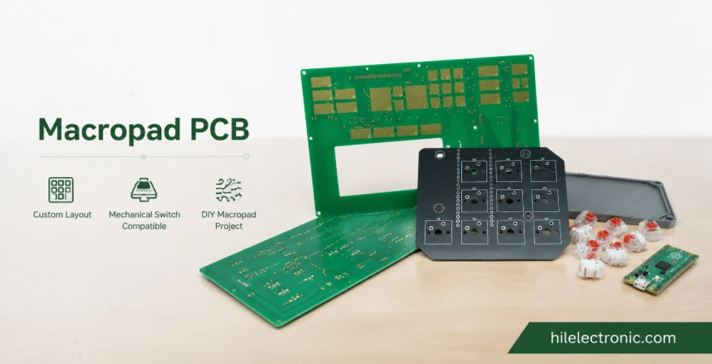
Macropad PCB Manufacturing & Custom PCBA
Table of contentsMacropad PCB Buying Guide and Quick...
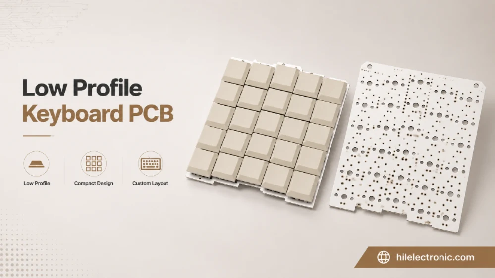
Low-Profile Keyboard PCB Manufacturing & Assembly
Table of contentsLow Profile and Choc Keyboard PCBA...
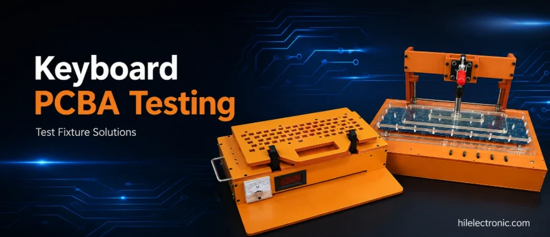
Keyboard PCBA Testing & Firmware Programming
Table of contentsKeyboard PCB Functional Testing Scope and...

Hall Effect Keyboard PCB Manufacturing & PCBA
Table of contentsHall Effect Keyboard PCB Buying...
How to get a quote for PCBs
Let us run DFM/DFA analysis for you and get back to you with a report.
You can upload your files securely through our website.
We require the following information in order to give you a quote:
-
- Gerber, ODB++, or .pcb, spec.
- BOM list if you require assembly
- Quantity
- Turn time
In addition to PCB manufacturing, we offer a comprehensive range of electronic services, including PCB design, PCBA (Printed Circuit Board Assembly), and turnkey solutions. Whether you need help with prototyping, design verification, component sourcing, or mass production, we provide end-to-end support to ensure your project’s success. For PCBA services, please provide your BOM (Bill of Materials) and any specific assembly instructions. We also offer DFM/DFA analysis to optimize your designs for manufacturability and assembly, ensuring a smooth production process.