
Back to blog
Cutting-Edge PCB Reverse Engineering Services

PCB Reverse Engineering
Reverse engineering in the electronics field is of great significance, especially in the circuit board industry. PCBs are the backbone of modern high-tech electronics, and understanding their inner workings through reverse engineering can transform innovation, replication, and troubleshooting. We will take an in-depth look at PCB reverse engineering, exploring its techniques, applications, and the critical role it plays in today’s technology landscape.
What is PCB Reverse Engineering?
PCB Reverse Engineering, short for Printed Circuit Board Reverse Engineering, is a meticulous process and methodology employed in the field of electronics to dissect, analyze, and recreate the design and functionality of a PCB without access to its original schematics, design files, or documentation. This practice involves reverse engineering techniques to unveil the inner workings of a PCB, including the placement of components, the routing of traces, the connections between various elements, and the overall electrical design.
The primary objective of PCB Reverse Engineering is to gain a deep understanding of an existing PCB, often when there is a lack of comprehensive documentation or when the original design files are unavailable. Engineers and technicians use this process to decipher how a PCB functions, troubleshoot issues, replicate or replace obsolete components, and make improvements or modifications to the original design.
PCB Reverse Engineering typically encompasses a range of tasks, including visual inspection, component identification, schematic generation, netlist extraction, and PCB layout reconstruction. Advanced techniques may involve X-ray or CT scanning to access internal details of the board, especially when it’s necessary to analyze multi-layer PCBs or identify hidden components and traces.
This practice is widely utilized in various industries, such as aerospace, automotive, telecommunications, consumer electronics, and defense, where PCBs play a critical role in the operation of complex systems and electronic devices. PCB Reverse Engineering serves as a valuable tool for ensuring the longevity of legacy systems, protecting intellectual property, and enabling cost-effective solutions for electronics maintenance and innovation.
Why Learn the Art of PCB Reverse Engineering?
Learning the art of PCB Reverse Engineering is a valuable skill that offers engineers and technicians a range of benefits, especially when differentiating it from PCB cloning. PCB Reverse Engineering involves understanding and recreating the working principle of a printed circuit board without producing an exact replica. Here are compelling reasons why mastering PCB Reverse Engineering is important:
Substitute Obsolete Components: PCB Reverse Engineering enables the identification and replacement of outdated components with cost-effective modern alternatives. Over time, semiconductor technology evolves rapidly, rendering original components obsolete or non-compliant with environmental regulations. By reverse engineering PCBs to schematics, engineers can enhance circuit functionality using readily available and economical state-of-the-art components.
Comprehensive Understanding: PCB Reverse Engineering is a valuable educational tool for gaining an in-depth understanding of technology. It allows engineers to deconstruct PCBs and create netlists, providing insights into circuit operation, component interconnections at various levels, layout features, semiconductor packaging, and system functionality. This knowledge contributes to mastery of technology and fosters opportunities for proposing improvements.
File Correction and Platform Migration: Existing PCB designs may have corrupted files that require modification or may need to transition to entirely new platforms. In such cases, having access to PCB design files, schematics, netlists, and bill of materials is essential for system updates. PCB Reverse Engineering becomes indispensable for rectifying errors in design files and facilitating platform migrations.
Design Replication: While exact replication of PCB designs through reverse engineering can be challenging, it is feasible. However, due to the complexity of modern multilayer PCBs, achieving absolute replication is cumbersome. Techniques like automated X-rays and photocopying may introduce deviations in the re-engineered circuit, impacting PCB functionality. It’s important to note that copyright regulations typically allow companies to replicate functionality rather than design. Disclosure of the new PCB details and identification of trace routing modifications and upgraded electronic components are essential when copying a design.
In essence, PCB Reverse Engineering empowers engineers to adapt, innovate, and overcome challenges related to legacy systems, component obsolescence, and quality assurance. It is a skill that provides valuable insights into technology, fosters education, supports system updates, and, when necessary, enables the replication of critical functionality. As the electronics industry continues to evolve, mastering the art of PCB Reverse Engineering becomes increasingly relevant and advantageous.

Manual PCB Reverse Engineering Process
Reverse engineering a PCB manually is a meticulous and essential process for gaining a comprehensive understanding of its design and functionality. This manual approach involves several systematic steps, each crucial in unraveling the intricacies of the PCB. Below is a detailed walkthrough of the manual PCB reverse engineering process:
Step 1: Component Identification
The initial step in manual PCB reverse engineering is the identification of electronic components present on the PCB. This entails meticulously recognizing and categorizing each component type, including resistors, capacitors, diodes, transistors, integrated circuits (ICs), connectors, inductors, and other elements. Acquiring knowledge of their names and classifications expedites the identification process.
IC Chip Identification:
In contemporary PCBs, IC chips are prevalent and often feature uniform black encapsulation. Identifying the unique alphanumeric markings on IC chips is imperative, as these markings serve as identifiers for locating datasheets and specifications online. Some manufacturers may deliberately obscure these markings to hinder reverse engineering.
SMD Resistor Coding:
Surface mount device (SMD) resistors, commonly found in modern PCBs, do not typically employ traditional color band schemes for identification. Instead, a standardized coding system such as the EIA marking code is utilized. Deciphering these codes can be challenging, but online resources and applications are available to assist in determining the resistor values based on the code.
Step 2: Data Acquisition
The subsequent phase in PCB reverse engineering involves data acquisition. To successfully reverse engineer a PCB, it is essential to obtain at least two identical PCB samples for comparative analysis. Additionally, detailed scanned images of the populated PCBs are indispensable, as they provide insights into component polarities and locations.
Comprehensive Information Gathering:
Collecting comprehensive information about component specifications, types, technical manuals, PCB assembly instructions, usage and maintenance data, and performance specifications is crucial. A meticulous visual inspection of the printed circuit board is also essential to identify any disparities between available data and the actual PCB.
Component Removal and PCB Cleaning:
Upon completing data collection, it is advisable to remove components from the PCB. Subsequently, clean the PCB thoroughly to remove solder residues and contaminants. Finally, employ compressed air to ensure the PCB is free from dirt and dust, providing a clear surface for analysis.
Step 3: Signal Analysis
Signal analysis is the most intricate phase of PCB reverse engineering, involving the mapping of interconnections, or traces, between components on the PCB. It is crucial to begin by identifying the PCB type, categorizing it as single layer, double layer, or multilayer, as this significantly impacts the complexity of the tracing process.
Single Layer PCBs:
Single layer PCBs have traces on one side and electronic components on the other. They primarily consist of through-hole components, simplifying the tracing of connections.
Double Layer PCBs:
Double layer PCBs have traces on both sides, with surface mount components on one side and through-hole components on the other. Traces often run beneath through-hole components and IC chips, making visual tracing impractical. A multimeter with continuity testing or an Ohm meter can be used to identify connections.
Multilayer PCBs:
Multilayer PCBs are the most intricate to trace, often featuring power traces in the middle layers. Reverse engineers must think like the PCB’s designer to navigate complex multilayer designs.
Systematic Tracing:
Initiate the tracing process by matching component pin connections one at a time to other pins. Begin with power supply traces, as their attachment points are typically known. Trace connections to voltage regulators and other components, referring to datasheets when necessary. Categorize and label components and traces as their functions are identified.
Mastering the manual PCB reverse engineering process is an ongoing endeavor that deepens your understanding of circuit design and decoding techniques. The ability to reverse engineer PCBs empowers engineers to troubleshoot, modify, or replicate electronic systems effectively, making it a valuable skill in various industries. PCBs’ increasing complexity ensures that the conversation surrounding PCB reverse engineering remains dynamic and continually evolving.

Automated PCB Reverse Engineering Process
Automated PCB reverse engineering is a sophisticated approach that leverages technology to streamline and enhance the process of dissecting and understanding complex printed circuit boards. This comprehensive guide explores the intricacies of automated PCB reverse engineering, providing a detailed insight into the methodologies and tools employed in this advanced field.
Utilize PCB Reverse Engineering Software:
Automated PCB reverse engineering begins with the utilization of specialized software tailored for this purpose. These software solutions are equipped with a plethora of features designed to expedite and enhance the reverse engineering process. Key functionalities include:
- Schematic Diagram Drawing: These tools have the capability to automatically generate schematic diagrams based on the PCB layout, offering a visual representation of the circuit’s design.
- Multilayer Circuit Board Design: As many PCBs feature multiple layers, the software excels in handling the intricacies of multilayered designs, ensuring accurate reconstruction.
- Drawing Generation: Automated drawing generation simplifies the documentation process, aiding engineers in creating precise and comprehensive design documents.
- Digital and Analog Circuit Simulation: Some advanced software tools provide simulation capabilities, enabling engineers to analyze the behavior of digital and analog circuits, furthering their understanding.
- Programmable Logic Semiconductor Design: For PCBs incorporating programmable logic devices, these software tools facilitate design, analysis, and integration into the reverse-engineered circuit.
Typically, the software operates by processing high-resolution images of both sides of the printed circuit board, automating initial tasks such as component identification and the retrieval and analysis of information related to these components.
Automated Component Detection Using Machine Vision:
Machine vision technology plays a pivotal role in the automation of PCB reverse engineering. Automated systems equipped with high-resolution cameras and advanced image processing algorithms can swiftly detect and identify components present on the PCB. These components include resistors, capacitors, integrated circuits, connectors, and more. Machine vision ensures rapid and precise component identification, significantly enhancing the efficiency of the reverse engineering process.
Data Collection and Analysis:
The heart of automated PCB reverse engineering lies in the comprehensive collection and analysis of technical documents associated with the components on the PCB. The process unfolds as follows:
- Image Segmentation: High-resolution images of the PCB are meticulously analyzed to identify distinct features of microchips and other components. This segmentation process generates regions corresponding to the chip packages.
- Optical Character Recognition (OCR): The segmented areas containing text, such as part numbers imprinted on integrated circuit packages, undergo Optical Character Recognition (OCR). OCR software extracts alphanumeric information from these images.
- Matching and Validation: Extracted part numbers are subjected to rigorous validation by comparing them against known manufacturer naming patterns and part numbers. This step serves to reduce false positives and ensure data accuracy.
- Web Search: Valid part numbers serve as keys to initiate web searches for associated technical documents, including datasheets. This search may encompass conventional search engines or specialized engines exclusively indexing datasheets.
- Document Retrieval: Relevant technical documents, such as datasheets, are automatically downloaded, and critical data such as pinout diagrams, feature descriptions, and pin signal tables are systematically extracted.
- Conversion to Structured Format: Technical documents often exist in PDF format; hence, they are converted into structured formats like XML. This transformation facilitates efficient data extraction and analysis.
- Filtering and Organization: Automated software proficiently filters out irrelevant documents, such as marketing brochures, based on predefined criteria like page count and matching keywords. The results are systematically organized into a well-structured database or file system.
Connection Analysis:
Once critical components are identified, and technical documents are meticulously analyzed, automated systems assist in probing and documenting the actual connections between components on the PCB. This crucial step is carried out using a multimeter, and the results are seamlessly integrated into the software’s comprehensive database.
Visualization and Reporting:
The processed data is presented through an intuitive graphical user interface, allowing engineers to access information efficiently and effectively. Furthermore, the software empowers engineers to create visually informative reports summarizing the findings. These reports serve as invaluable tools for communication, enabling the seamless exchange of insights with other stakeholders, including engineering teams and customers.
Automated PCB reverse engineering represents the pinnacle of efficiency and accuracy in dissecting and comprehending intricate printed circuit boards. This advanced approach amalgamates machine vision, sophisticated data analysis, and specialized software to streamline the reverse engineering process significantly. The outcome is a comprehensive understanding of PCB designs, making automated PCB reverse engineering an indispensable asset across a spectrum of industries requiring precise PCB analysis and modification.

Advanced PCB Reverse Engineering Techniques
The reverse engineering of Printed Circuit Boards (PCBs) is a complex process involving the extraction of the internal structure and interconnections of the board’s layers. This process can be accomplished through either non-destructive or destructive methods, each with its own set of advantages and applications.
Non-Destructive PCB Reverse Engineering Techniques
X-ray Tomography:
Non-destructive PCB reverse engineering techniques have gained prominence in recent years due to their cost-effectiveness, reduced processing times, and the potential for implementing trust verification mechanisms.
X-ray Tomography stands out as a leading non-destructive method in PCB reverse engineering. It allows for the comprehensive imaging of the entire PCB without the need for physical delayering, making it particularly advantageous for preserving PCB integrity.
How X-ray Tomography Works: X-ray tomography involves the acquisition of a series of two-dimensional (2D) X-ray images of the PCB from various angles. These 2D images are subjected to sophisticated mathematical algorithms such as center slice theory and direct Fourier transform to reconstruct a detailed three-dimensional (3D) image of the PCB’s internal structure.
Several critical parameters influence the quality of X-ray tomography:
- Source Power: This parameter relates to the penetration depth and X-ray energy.
- Detector Objective: It dictates the achievable resolution range and field of view.
- Filtering: The use of filters regulates the dose, allowing higher-energy X-rays to pass through.
- Distance between Detector and Source: This parameter has an inverse relationship with the number of counts.
- Number of X-ray Projections: It determines the angular increment for each rotation of the sample during tomography.
- Exposure Time: This parameter is linearly correlated with counts and significantly affects the overall scanning time and cost.
Optimizing these parameters, depending on the region of interest within the PCB, is crucial for achieving the desired signal-to-noise ratio and pixel size.
Once the 3D image is reconstructed, further analysis can be performed to examine the interior and exterior structures of the PCB. Techniques such as beam hardening correction and center shift tuning may be applied to enhance the image quality.
Non-destructive techniques like X-ray tomography offer several advantages, including the preservation of PCB integrity, reduced costs, and the potential for implementing trust verification tests, which can be vital in critical applications.
Destructive PCB Reverse Engineering Techniques
Destructive reverse engineering techniques are typically applied to multilayered PCBs and involve a series of well-defined steps, including solder mask removal, delayering, and imaging.
Solder Mask Removal:
The initial step in destructive PCB reverse engineering is the precise removal of the solder mask from the PCB. This process aims to reveal the underlying copper traces while minimizing damage, ensuring a clear view of the traces.
Solder mask removal is typically performed after removing all components from the PCB. Various techniques can be employed for this purpose, including:
- Sandpaper
- Abrasive Blasting
- Fiberglass Scratch Brushes
- Chemical Methods
- Laser Technology
Each technique is chosen based on the specific requirements and constraints of the reverse engineering project.
Delayering:
Following the successful removal of the solder mask, the next critical step is delayering. Delayering involves the physical removal of layers to access the internal copper layers of multilayered PCBs. This process must be meticulously performed after all components have been carefully extracted from the PCB.
Several methods for PCB delayering may be applied, including:
- X-ray Delayering: Utilizing X-ray technology to selectively remove layers while preserving the underlying structures.
- Sandpaper Delayering: A precise manual method involving the controlled removal of layers using fine sandpaper.
- Dremel Tool Delayering: Employing a Dremel tool with precision control to remove layers incrementally.
- Surface Grinding Delayering: A controlled surface grinding process to expose internal layers.
- CNC Milling Delayering: Computer Numerical Control (CNC) milling machines are used to selectively remove layers, ensuring accuracy and control.
The choice of delayering method depends on factors such as the PCB’s complexity, the desired level of precision, and the available equipment and expertise.
Imaging:
Once delayered, the next imperative step is to capture individual images of each layer of the multilayer PCB. Importantly, this imaging process should ideally be non-destructive and capable of providing detailed layer-by-layer information.
Imaging during PCB reverse engineering can be achieved through the use of:
- X-ray Imaging (2D): Employing X-ray technology to capture detailed images of each layer without compromising the structural integrity of the PCB.
- Computerized Tomography (3D X-ray): A sophisticated technique that generates three-dimensional images of the PCB, allowing for comprehensive layer analysis.
Both methods offer distinct advantages and are chosen based on the specific project requirements and equipment availability.
In summary, PCB reverse engineering encompasses a spectrum of techniques, ranging from non-destructive methods like X-ray tomography to destructive approaches involving solder mask removal, delayering, and imaging. The selection of the appropriate technique depends on factors such as project objectives, budget, time constraints, and the intricacy of the PCB under investigation.

Applications of PCB Reverse Engineering
PCB reverse engineering techniques find valuable applications in various situations where the original PCB design or documentation is unavailable or insufficient. Below are some common scenarios where PCB reverse engineering is applied:
- Obsolete Devices with Lost Artwork: When dealing with older devices that have become obsolete and where the original PCB artwork or documentation is no longer accessible, reverse engineering can be employed to recreate the PCB layout and design. This is particularly useful for ensuring continued support and maintenance of legacy equipment.
- WEEE/RoHS Compliance Redesign: Devices that need to comply with environmental regulations such as the Waste Electrical and Electronic Equipment (WEEE) directive or the Restriction of Hazardous Substances (RoHS) directive may require PCB redesign. Reverse engineering helps in creating compliant PCB layouts while maintaining the functionality of the original device.
- Obsolete Products without Circuit Diagrams: In cases where product designs lack comprehensive circuit diagrams or schematics, reverse engineering can be utilized to reconstruct the circuitry. This is essential for troubleshooting, repairs, or product improvements.
- Migration from Through-Hole to SMD Components: As technology evolves, there is often a need to migrate from through-hole components to Surface Mount Device (SMD) components for reasons like size reduction, improved performance, or cost efficiency. PCB reverse engineering aids in transitioning to SMD technology while preserving the original circuit’s functionality.
- Adoption of Emerging Technologies: When incorporating new and emerging technologies into existing systems, it’s crucial to integrate them seamlessly while maintaining the logic and core features of the current PCBs. Reverse engineering facilitates this process by allowing for the adaptation of modern components and technologies.
- Design Modifications: PCB reverse engineering is employed for making design modifications or improvements to existing boards. This could involve adding new features, optimizing the layout for better performance, or addressing known issues in the original design.
- Enhancing Functionalities: Devices that require additional functionalities, such as increased processing power, connectivity options, or expanded capabilities, can benefit from PCB reverse engineering. It enables the integration of new components and circuitry to enhance overall functionality.
- Maintenance and Support on Older PCBs: For older PCBs that are still in use but lack adequate documentation or replacement parts, reverse engineering ensures the availability of support and maintenance. This is particularly valuable for industries where equipment longevity is critical, such as aerospace or industrial automation.
- Improved Performance: PCB reverse engineering can be employed to analyze and optimize existing PCB layouts for improved performance, reduced noise, or enhanced reliability. This can result in more efficient and reliable electronic systems.
- Lower Life-Cycle Costs and Reduced System Cost: By reverse engineering PCBs, organizations can extend the life cycle of their products, reduce maintenance costs, and potentially lower overall system costs. This is achieved by keeping older systems operational and minimizing the need for complete redesigns.
Conclusion
PCB reverse engineering is a valuable and versatile process that allows for the reconstruction and analysis of printed circuit boards when the original designs or documentation are unavailable or insufficient. Whether it involves recreating obsolete devices, ensuring compliance with environmental regulations, or adapting to emerging technologies, reverse engineering plays a crucial role in maintaining, improving, and optimizing electronic systems.
The complexity of modern PCBs necessitates a thorough understanding of components, connections, and layouts. Professional reverse engineers bring expertise and experience to the table, enabling organizations to successfully navigate the intricacies of PCB reverse engineering. By leveraging the services of skilled professionals, companies can streamline electronic production services, address complex requirements, and ensure the continued functionality and longevity of their electronic systems.
In a rapidly evolving technological landscape, PCB reverse engineering remains an indispensable tool for industries that rely on electronics, providing solutions to challenges related to legacy equipment, design modifications, compliance, and performance enhancement. It empowers organizations to adapt, innovate, and thrive in the world of electronics.

Recommended Posts

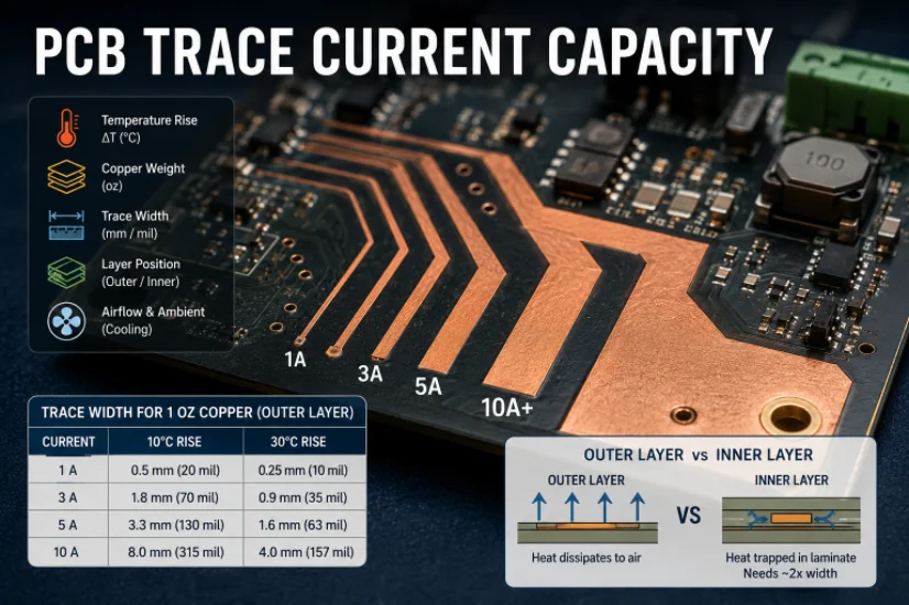
PCB Current Calculator: Sizing Trace Width and Vias with the IPC-2221 Formula
Figure 1. Pcb Current Calculator reference image for PCB...

Microphone PCB Design: How the Board Itself Shapes Your Audio Quality
Figure 1. Microphone Pcb reference image for PCB...
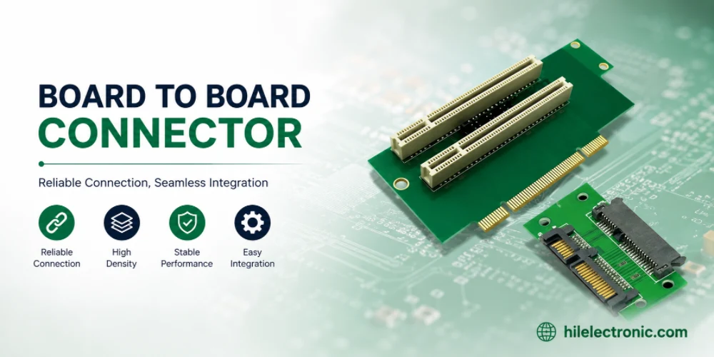
Board-to-Board Connector: Types, Specifications, and How to Select One
Figure 1. Board To Board Connector reference image for PCB...
PCB Trace Width Calculator: How to Size Traces for Current, Voltage Drop, and Impedance
Figure 1. A PCB trace width calculator is a starting point...