
TMM13i PCB Manufacturing
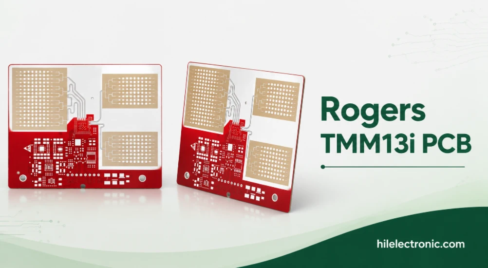
TMM13i PCB manufacturing is aimed at ultra-compact RF geometry, where tolerance allocation can become part of the electrical design budget. The useful manufacturing question is which dimensions are truly critical and how those dimensions will be verified. TMM13i is used when a microwave circuit must become very small and the designer needs a nearly isotropic, very high-Dk thermoset substrate. The material can compress resonators, filters, patch antennas and matching networks, but the electrical benefit shifts attention to machining, datums, finish thickness and production change control.
Highleap Electronics manufactures PCBs using TMM13i material and PCB assemblies for compact RF modules. The build is treated more like a precision microwave component than a general printed circuit board.
The TMM13i page focuses on ultra-miniature RF construction and production change control. Once the prototype is qualified, the approved material construction, critical dimensions, finish, housing interfaces and test method should become the reference for repeat builds.
What TMM13i Changes in an Ultra-Miniature RF Design
Very high Dk reduces guided wavelength and allows distributed structures to occupy less area. Nearly isotropic behavior is useful where the electromagnetic field extends through several directions and interacts with a housing, cavity or nearby metal. The tradeoff is that a small absolute error becomes a large percentage of the final feature.
Tolerance must be allocated as an RF budget
The acceptable frequency or impedance shift should be divided among material Dk, thickness, etch, machining, finish, housing and assembly. Applying a single generic PCB tolerance does not show which variable is consuming the margin.
| Error source | Why it matters | Control |
|---|---|---|
| Resonator length | Directly shifts center frequency | Finished-dimension inspection |
| Coupling gap | Changes bandwidth and coupling | Capability review and optical measurement |
| Substrate thickness | Changes capacitance and field distribution | Exact construction and incoming verification |
| Finish thickness | Meaningful relative to very small pads and gaps | Selective finish and thickness control |
| Housing spacing | Loads the strongly confined field | Common datums and assembled correlation |
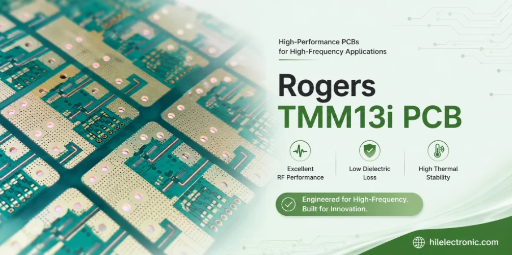
Material scope: the Rogers product name is used to identify the laminate specified for the PCB build. Highleap Electronics provides PCB fabrication and assembly, while the laminate is sourced and verified separately.
Precision Machining and Metallization for TMM13i Modules
The RF artwork, routed outline, cavities, mounting features and housing should use a common datum scheme. Highleap reviews the machining sequence so that routing or drilling does not destroy the reference needed for later inspection. Small features may require dedicated support and tool selection to maintain edge quality.
Bond pads and selective finishes
Wire-bond pads, die-attach areas and small coupling features should not receive an unspecified finish. The finish must match the assembly method, and its thickness should be included in the geometry budget. Selective finishing can keep high-Q RF structures free from unnecessary metal while providing suitable bondability elsewhere.
- Rank the frequency-setting dimensions before tolerance negotiation.
- Use common datums for artwork, machining and the module housing.
- Measure finished features rather than relying only on artwork values.
- Define selective metallization and bond-pad cleanliness.
- Control lot, thickness and copper changes through formal approval.
- Validate the substrate in the assembled housing, not only as an open board.
Highleap’s wire-bonding PCB guidance is relevant when TMM13i becomes the base of a hybrid microwave module.
Temperature, Housing and Mechanical Constraints
TMM13i can compete with ceramic substrates in some compact microwave products, but it is not a drop-in ceramic replacement. Mechanical stiffness, metallization, thermal conductivity, machining and assembly differ. The design should compare the complete module rather than Dk alone.
Where the material fits
Typical uses include miniature resonators, narrowband filters, compact patch antennas, matching networks and tightly packaged microwave modules. The material is less suitable when broad bandwidth and generous manufacturing geometry are more important than size.
For a wider comparison with ceramic approaches, see ceramic PCB versus organic PCB.
Production Change Control for TMM13i PCB
At very high Dk, an apparently small change in thickness, copper, finish or machining can move the RF response. The approved build should therefore identify the exact material construction, critical dimensions, finish, housing interface and qualification data. Any substitution should be reviewed against the released model.
Prototype and qualification package
Highleap can provide first-article dimensional reports, cross-sections, electrical tests and customer-defined RF correlation. Prototype, low-volume and repeat production can be followed by component assembly when the bond, die-attach or SMT process is defined. Highleap reviews fine features, pad geometry, plated holes, metallization and dimensional control around the compact RF area. The first article should create a record of the critical features so repeat production has measurable acceptance points. Exact material property values should be checked against the current supplier documentation for the specified grade and construction.
Provide the TMM13i RF model assumptions, critical dimensions, machining drawing and housing. Highleap will review the tolerance budget and propose a qualification route appropriate to the module.
TMM13i questions
Is TMM13i simply a smaller version of TMM4? No. The very high Dk changes geometry, tolerance sensitivity and housing interaction.
Can the finish be changed after tuning? A finish change can alter small pads and gaps, so it should be reviewed and requalified. For a TMM13i quotation, provide the exact grade, stackup, smallest features, board thickness, finish, quantity and RF validation requirements. The quotation should reflect the precision of the released construction.

Recommended Posts

TMM4 Filter PCB Manufacturing
TMM4 filter PCB manufacturing is controlled by the...

TMM3 PCB Manufacturing for RF Modules
TMM3 PCB manufacturing is most useful where the RF module...

TMM6 PCB Fabrication
TMM6 fabrication is the process-control page for a mid-Dk...

TMM10 PCB Manufacturing for Compact RF Designs
Table of contentsHow TMM10 Shrinks RF StructuresTMM10 vs...
How to get a quote for PCBs
Let’s run DFM/DFA analysis for you and get back to you with a report. You can upload your files securely through our website. We require the following information in order to give you a quote:
-
- Gerber, ODB++, or .pcb, spec.
- BOM list if you require assembly
- Quantity
- Turn time
For PCBA services, please provide your BOM (Bill of Materials) and any specific assembly instructions. We also offer DFM/DFA analysis to optimize your designs for manufacturability and assembly, ensuring a smooth production process.