
Basic Rules of PCB Design for High-Quality Circuit Boards

Printed Circuit Board (PCB) design is a cornerstone of modern electronic product development, requiring a nuanced understanding of electrical engineering, electromagnetic theory, and manufacturing limitations. As electronics become more sophisticated, the complexity of PCB design has increased, making adherence to specific design rules and best practices crucial. These rules ensure functionality, manufacturability, reliability, and cost-effectiveness. A well-designed PCB often defines a product’s success in terms of performance and durability. This article provides an in-depth examination of the critical rules of PCB design, emphasizing technical aspects and professional considerations.
1. Layer Stack-Up Rules
Layer stack-up refers to the organization and arrangement of the conductive layers, insulating layers, and substrates within a PCB. Proper stack-up planning is essential for signal integrity, electromagnetic interference (EMI) control, and impedance matching.
-
Symmetrical Layer Stack-Up: For mechanical stability and to prevent warping during thermal cycles, maintain a symmetrical stack-up around the PCB’s centerline. A balanced stack-up reduces mechanical stress, especially in multilayer boards.
-
Reference Planes: Signal layers should be adjacent to continuous reference planes (ground or power planes). This minimizes EMI by providing a low-impedance return path, which is critical for high-speed signals.
-
Dielectric Material Selection: The dielectric constant (Dk) and loss tangent (Df) of insulating layers influence signal propagation speed and attenuation. High-frequency applications often require low-loss materials like Rogers or Megtron rather than standard FR-4 to reduce signal degradation.
-
Characteristic Impedance Control: Transmission lines should be designed to maintain characteristic impedance, usually between 50 to 75 ohms for single-ended signals or 90 to 100 ohms for differential pairs. The impedance depends on trace width, spacing, and dielectric properties. Field solvers, such as Ansys HFSS or CST Studio, can assist in accurately modeling and verifying impedance requirements.
2. Component Placement Rules
Component placement dictates not only the performance of a PCB but also its manufacturability and thermal management.
- Functional Block Organization: Place components in logical blocks based on their function, aligning with signal flow. For example, high-speed components (processors, memory) should be positioned centrally, with supporting components (decoupling capacitors, power regulators) surrounding them to reduce signal path lengths.
- Thermal Management Considerations: High-power components such as MOSFETs, voltage regulators, and processors should be spaced adequately to facilitate heat dissipation. Use thermal vias under these components to transfer heat from the component pad to internal or external heat sink layers.
- Decoupling Capacitor Placement: Bypass and decoupling capacitors should be placed within 0.1 inches (2.5 mm) of IC power pins. This minimizes the loop area, reducing high-frequency noise by effectively decoupling power supply fluctuations.
- Clearances and Creepage Distances: For high-voltage designs, ensure proper creepage and clearance distances between components to prevent arcing or dielectric breakdown. IPC-2221 standards recommend specific clearances based on operating voltage and environmental factors.
3. Trace Routing Rules
Routing traces is one of the most intricate parts of PCB design, especially in high-speed and high-frequency circuits.
-
Controlled Impedance Traces: Controlled impedance is crucial for signal integrity, especially in high-speed designs. Trace width, spacing, and the distance to reference planes should be carefully calculated to meet impedance requirements. Tools like IPC-2141 can assist in calculating appropriate trace widths based on material properties.
-
Differential Pair Routing: Differential pairs should maintain equal trace lengths and consistent spacing to preserve differential impedance, critical for USB, HDMI, and Ethernet protocols. Length mismatch in differential pairs should be kept under 5 mils to prevent timing skew.
-
Via Usage in High-Speed Signals: Excessive vias can introduce impedance discontinuities, adding parasitic capacitance and inductance. For sensitive signals, consider minimizing via transitions or using back-drilled vias, which reduce via stub length, mitigating signal reflection and loss.
-
Stub Length Minimization: Stubs, or unterminated traces, act as antennas that can cause signal reflections. In RF designs, routing traces without stubs and utilizing blind or buried vias help to reduce reflection.
-
Trace Width for Current Carrying Capacity: Use IPC-2152 standards to determine trace widths based on current-carrying requirements. For internal layers, a typical guideline is 10 mils per ampere, while external layers require around 15 mils per ampere to avoid excessive temperature rise.
For production planning, it also helps to compare this topic with PCB design review and PCB fabrication capability before finalizing the fabrication or assembly package.

Circuit Design,PCB Design
4. Design for Manufacturability (DFM) Rules
DFM ensures that the PCB design can be produced cost-effectively without errors.
-
Annular Ring Specifications: The annular ring (the conductive area around via holes) should be large enough to accommodate potential drill misalignments. For plated-through holes, IPC recommends a minimum annular ring of 10 mils, though high-density designs may allow smaller rings if manufacturing capabilities support it.
-
Solder Mask and Paste Mask Guidelines: Proper solder mask clearance is critical to avoid solder bridging. The recommended mask expansion (gap between pad and solder mask) is 2-4 mils, depending on design tolerances and manufacturing processes.
-
Component Pad Sizes and Via-in-Pad: Pads should be sized to match the component lead size, typically with 0.1 to 0.2 mm additional diameter for plated-through holes. If using via-in-pad, ensure they are filled and capped to prevent solder wicking, which can lead to weak solder joints.
-
Copper-to-Edge Clearances: To avoid delamination and prevent accidental shorting during depaneling, copper features should be set back from the board edge by at least 0.5 mm.
5. Signal Integrity (SI) and Crosstalk Reduction Rules
Signal integrity (SI) is vital for high-speed designs, where digital signals need to transition cleanly without distortion.
-
Right-Angle Trace Avoidance: Right-angle bends can cause signal reflections and EMI issues. For critical signals, use 45-degree bends or, ideally, curve the traces to maintain consistent impedance.
-
Ground Return Paths: Signal traces should have a continuous ground return path to reduce loop inductance and EMI. Ensure that signal layers are close to ground planes, ideally adjacent layers in the stack-up.
-
Spacing to Reduce Crosstalk: Maintain a spacing of at least 3x the trace width between high-speed traces to reduce capacitive and inductive coupling, which can cause crosstalk.
-
Stub Minimization and Termination: In RF and high-speed digital designs, avoid stubs by routing signals with proper termination. Where unavoidable, stubs should be as short as possible to reduce reflection.
6. Power Integrity (PI) Rules
Maintaining stable power delivery is essential for digital and analog circuits, especially with increasing power densities in modern PCBs.
-
Power and Ground Planes: Solid power and ground planes provide a low-impedance path, reducing voltage drops and noise. These planes also act as a heat spreader, improving thermal management.
-
Decoupling Network Design: Use a combination of bulk and high-frequency decoupling capacitors near each IC. Bulk capacitors (10 μF or larger) provide energy during transient events, while high-frequency capacitors (0.01–0.1 μF) reduce high-frequency noise.
-
Minimizing Power Supply Loop Area: Keeping power and ground traces close together reduces loop area, which in turn minimizes radiated EMI. Multilayer boards benefit from placing power and ground planes adjacent to each other.
-
Power Integrity Modeling: Power integrity simulations (e.g., using software like Ansys SIwave) can predict voltage ripple and identify hotspots, helping optimize decoupling placement and plane design.
7. Thermal Management Rules
As devices consume more power, thermal management becomes increasingly important to prevent overheating and ensure reliable operation.
-
Thermal Via Arrays: High-power components, such as FPGAs, should have thermal via arrays to transfer heat from component pads to internal or external heat spreaders. Thermal vias are typically filled with epoxy or capped to ensure solderability.
-
Heat Sinks and Heat Spreaders: In high-power designs, attach heat sinks or heat spreaders to components that exceed safe temperature thresholds. Some PCBs may require embedded heat pipes or metal-core substrates for optimal cooling.
-
Convection and Forced Airflow: Arrange components to encourage natural convection or optimize forced airflow across high-power areas. For high-density designs, place heat-sensitive components away from heat sources.
8. Testing and Inspection Rules
Testing and inspection help verify PCB functionality and quality before full production.
-
Test Point Accessibility: Add test points for critical nodes to facilitate in-circuit testing (ICT) and debugging. Ensure test points are placed on accessible sides and are compatible with test probes.
-
AOI and X-Ray Inspection Requirements: Automated Optical Inspection (AOI) detects solder and component placement defects, while X-ray inspection is critical for boards with Ball Grid Array (BGA) packages, where solder joints are obscured. Ensure that layout adheres to AOI guidelines for clear visual inspection.
-
Boundary Scan and JTAG: For digital circuits, boundary scan (IEEE 1149.1 JTAG) provides a method to test interconnections without direct probe access. Integrate JTAG test points to facilitate testing, especially in dense or multilayer boards.
Conclusion
Following these essential rules in PCB design is critical to developing high-quality, reliable, and manufacturable printed circuit boards. With increasing design complexities, the guidelines provided here ensure that each phase—from layer stack-up to testing—meets industry standards.
By adhering to these principles, designers can minimize errors, reduce production costs, and enhance the performance and durability of their PCBs.
For a truly seamless experience, partner with us for comprehensive PCB solutions. Our team of skilled PCB designers can assist you with design, manufacturing, and assembly—all under one roof. Choose us for your electronic needs and enjoy a streamlined, one-stop service that delivers exceptional quality and reliability!
Get a Free PCB & PCBA Quote

Recommended Posts
FR408HR PCB Manufacturing Process and Multilayer Reliability
FR408HR multilayer reliability is created by the complete...
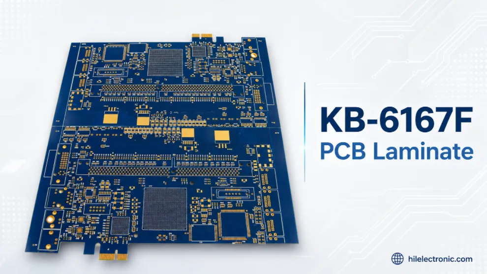
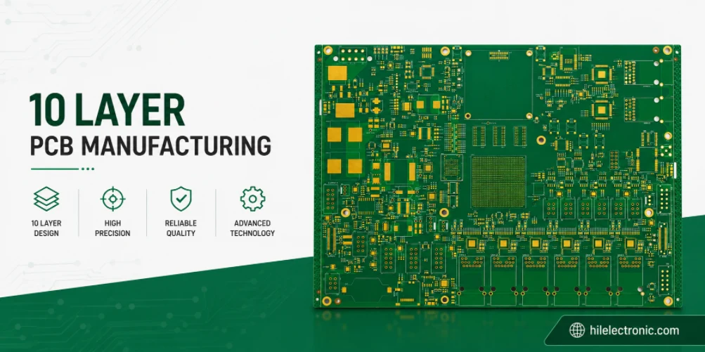
KB-6167F PCB Laminate for High-Tg Multilayer PCB Manufacturing
KB-6167F PCB laminate is used when a multilayer PCB needs...
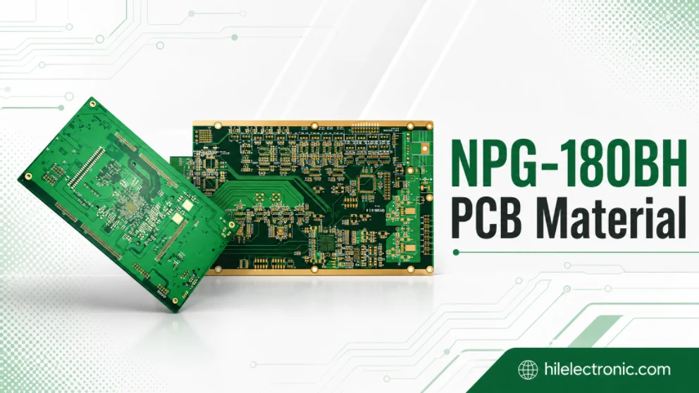
NPG-180BH PCB Material for Automotive and High-Reliability PCB Manufacturing
NPG-180BH PCB material is a Nan Ya halogen-free, high-Tg,...
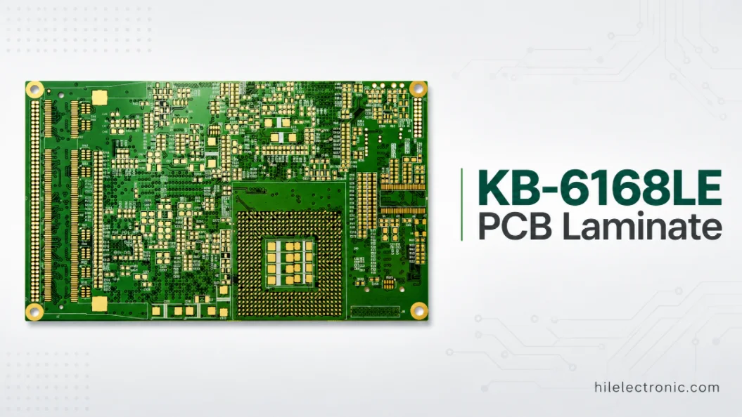
KB-6168LE PCB Laminate for Low Z-CTE Multilayer PCB Manufacturing
KB-6168LE PCB laminate is a Kingboard high-Tg, anti-CAF,...
How to get a quote for PCBs
Let us run DFM/DFA analysis for you and get back to you with a report.
You can upload your files securely through our website.
We require the following information in order to give you a quote:
-
- Gerber, ODB++, or .pcb, spec.
- BOM list if you require assembly
- Quantity
- Turn time
In addition to PCB manufacturing, we offer a comprehensive range of electronic services, including PCB design, PCBA (Printed Circuit Board Assembly), and turnkey solutions. Whether you need help with prototyping, design verification, component sourcing, or mass production, we provide end-to-end support to ensure your project’s success. For PCBA services, please provide your BOM (Bill of Materials) and any specific assembly instructions. We also offer DFM/DFA analysis to optimize your designs for manufacturability and assembly, ensuring a smooth production process.