
Signal Attenuation in High-Speed PCBs: Causes, Analysis, and Mitigation Strategies

1. Introduction: Definition and Importance of Signal Attenuation
Signal attenuation refers to the progressive reduction of signal strength as electrical energy propagates through a PCB transmission line. In high-speed digital and RF circuits, this phenomenon manifests as decreased voltage amplitude, degraded rise times, and diminished signal-to-noise ratios at the receiver end.
1.1 Why Signal Attenuation Matters for Signal Integrity
Excessive signal attenuation directly compromises signal integrity by causing waveform distortion, eye diagram closure, and elevated bit error rates. As data rates increase into the multi-gigabit range, even moderate attenuation can render a channel unusable, making loss management a primary design constraint.
1.2 Scope of This Article
This article examines the factors that cause signal attenuation in high-speed PCB designs and presents practical strategies to minimize transmission losses. The focus remains on PCB-specific considerations, from material selection through layout optimization to compensation techniques.
2. Underlying Physics of Signal Attenuation
2.1 Transmission Line Model and Attenuation Expression
PCB traces operating at high frequencies behave as distributed transmission lines rather than simple conductors. Signal attenuation along these lines is quantified in decibels per unit length (dB/inch or dB/mm), representing the logarithmic ratio of input to output power. Total attenuation comprises two primary components: conductor loss and dielectric loss, each with distinct frequency dependencies.
2.2 Conductor Loss in High-Speed PCBs
Resistance and Skin Effect
At DC and low frequencies, conductor loss depends primarily on bulk copper resistance. However, as frequency increases, the skin effect confines current flow to an increasingly thin layer near the conductor surface. This effective reduction in cross-sectional area raises AC resistance, causing conductor loss to scale approximately with the square root of frequency.
Surface Roughness Effects
Copper foil surface roughness further exacerbates conductor loss at high frequencies. When the skin depth approaches the roughness dimension, current must travel a longer effective path along the uneven surface. Smoother copper treatments such as VLP (Very Low Profile) or HVLP foils reduce this additional loss contribution significantly.
2.3 Dielectric Loss Mechanisms
Loss Tangent and Energy Absorption
Dielectric loss arises from the polarization response of the PCB substrate material to alternating electric fields. The loss tangent (Df or tan δ) quantifies this energy dissipation, with higher values indicating greater signal absorption. Unlike conductor loss, dielectric loss increases linearly with frequency, making it the dominant attenuation mechanism at multi-gigahertz rates.
High-Frequency Dielectric Behavior
At elevated frequencies, dielectric loss often exceeds conductor loss as the primary attenuation source. Substrate materials exhibit frequency-dependent dielectric properties, and accurate loss prediction requires characterizing Dk and Df across the operating bandwidth rather than relying on single-frequency datasheet values.

3. Key Causes of Signal Attenuation in High-Speed PCB Design
3.1 Frequency and Signal Path Length
Signal attenuation increases with both operating frequency and physical trace length. Higher frequency components within a signal spectrum experience greater losses, causing frequency-dependent amplitude roll-off. Long routing paths accumulate these losses, making path length minimization a fundamental design objective for high-speed channels.
3.2 Substrate Material Dk/Df Performance
The dielectric constant (Dk) and dissipation factor (Df) of PCB substrate materials significantly influence signal attenuation. Standard FR-4 exhibits relatively high loss tangent values (0.020–0.025), while advanced low-loss laminates such as Megtron, Rogers, or Isola materials offer Df values below 0.005. Material selection directly determines the achievable channel length at a given data rate.
3.3 Trace Geometry and Layout Considerations
Trace width, thickness, and length all affect attenuation magnitude. Narrower traces exhibit higher resistance and greater conductor loss. Sharp corners and unnecessary bends introduce impedance discontinuities and localized field concentrations. Optimized trace geometry balances impedance control requirements against loss minimization objectives.
3.4 Crosstalk and Return Path Quality
Crosstalk between adjacent traces and discontinuities in reference planes degrade effective signal amplitude at receivers. Poor return path routing increases loop inductance and creates common-impedance coupling. These effects compound direct attenuation losses, further reducing signal margins.
3.5 Via Transitions and Layer Changes
Vias introduce parasitic inductance and capacitance that create localized impedance mismatches. Each layer transition adds insertion loss from these discontinuities. High-speed designs require careful via optimization, including back-drilling, via-in-pad techniques, or blind/buried via structures to minimize transition losses.
4. Analysis and Measurement of Signal Attenuation
4.1 Vector Network Analyzer Frequency-Domain Measurements
Vector network analyzers (VNAs) provide the standard method for characterizing PCB channel attenuation. S-parameter measurements, particularly S21 (insertion loss), quantify frequency-dependent transmission losses across the operating bandwidth. VNA techniques enable accurate loss attribution between conductor and dielectric mechanisms.
4.2 Simulation Tools for Design-Stage Analysis
Electromagnetic field solvers and transmission line simulators predict attenuation before fabrication. These tools model frequency-dependent losses, generate eye diagrams, and evaluate channel performance against compliance masks. Pre-layout simulation guides material selection and geometry optimization decisions.
4.3 Simulation Accuracy and Measurement Correlation
Simulation accuracy depends on precise material characterization and geometric modeling fidelity. Discrepancies between simulated and measured results often arise from manufacturing tolerances, incomplete roughness models, or frequency-dependent material property variations. Correlation studies between simulation and test coupons establish confidence in predictive models.
5. Design Strategies for Mitigating Signal Attenuation
5.1 PCB Material Selection for Low Loss
Selecting substrate materials with low Dk and Df values directly reduces dielectric loss. Low-loss laminates become essential when channel lengths exceed loss budgets with standard materials. Cost-performance tradeoffs guide material selection, with hybrid stackups using premium materials only for critical signal layers offering practical compromises.
5.2 Controlled Impedance and Stackup Design
Maintaining controlled impedance throughout the signal path minimizes reflections that compound attenuation effects. Stackup design positions high-speed signal layers adjacent to continuous reference planes, ensuring low-inductance return paths. Consistent dielectric thickness and impedance control reduce discontinuity-induced losses.
5.3 Trace Geometry and Routing Optimization
Wider traces reduce conductor loss where impedance constraints permit. Minimizing trace length through direct routing and reduced layer transitions decreases cumulative attenuation. Avoiding acute-angle bends and maintaining smooth transitions preserves signal amplitude.
5.4 Attenuation Compensation Techniques
Pre-emphasis at transmitters boosts high-frequency signal components to offset frequency-dependent channel losses. Equalization at receivers applies inverse channel response to restore attenuated frequency content. These techniques extend achievable channel reach beyond passive loss limits.
5.5 Termination Matching and Noise Control
Proper termination matching at driver and receiver ends eliminates reflections that degrade signal amplitude. Series, parallel, and AC termination strategies address different impedance matching requirements. Clean power distribution and shielding techniques prevent noise coupling that reduces effective signal margins.
6. Considerations for Typical High-Speed Designs
High-speed serial interfaces such as PCIe Gen4/5, USB4, and 100G+ Ethernet operate at frequencies where signal attenuation dominates design constraints. These protocols specify maximum channel insertion loss budgets that directly determine allowable trace lengths and material requirements. RF and mmWave applications impose even more stringent loss constraints.
At multi-gigahertz frequencies, material and geometry decisions require careful analysis of loss-frequency tradeoffs. Design teams must balance cost against performance, selecting the minimum material grade that satisfies channel loss budgets while applying compensation techniques to maximize achievable reach.
7. Conclusion
Signal attenuation in high-speed PCBs results from the combined effects of conductor resistance, skin effect, surface roughness, and dielectric absorption. Frequency, path length, material properties, trace geometry, and transition quality all contribute to total channel loss.
Effective attenuation management requires a multi-dimensional approach encompassing material selection, impedance-controlled stackup design, optimized routing, and electronic compensation techniques. Accurate simulation and measurement correlation ensures designs meet loss budgets before production.
Future high-speed designs will demand continued advances in low-loss materials, smoother copper treatments, and more sophisticated compensation algorithms as data rates push further into the multi-tens-of-gigahertz regime.

Recommended Posts
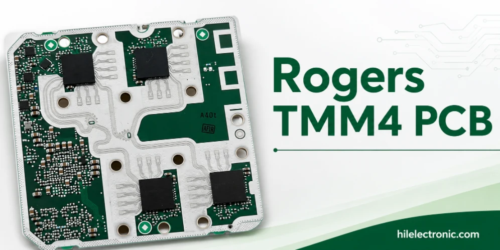
Rogers TMM4 PCB Manufacturer for Compact Microwave Filters
TMM4 is most useful when a microwave circuit must become...
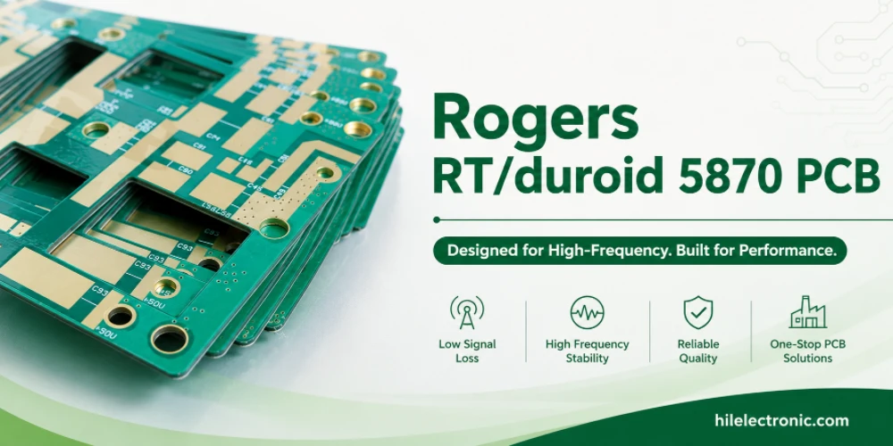
RT/duroid 5870 PCB Manufacturer for Low-Loss PTFE RF Circuits
RT/duroid 5870 is chosen when the RF path needs low loss,...
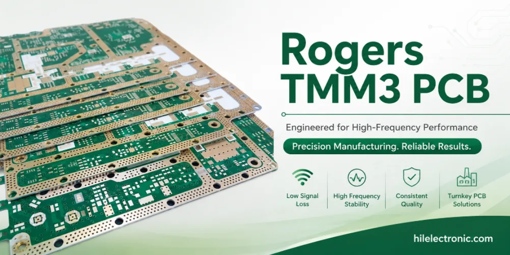
Rogers TMM3 PCB Manufacturer for Mechanical RF Modules
TMM3 is selected when an RF circuit must behave as part of...
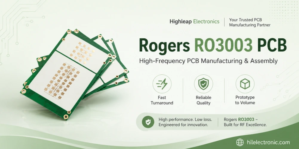
Rogers RO3003 PCB Manufacturer for Automotive Radar and mmWave Modules
A 77 GHz radar board is purchased as a working sensor...
How to get a quote for PCBs
Let‘s run DFM/DFA analysis for you and get back to you with a report. You can upload your files securely through our website. We require the following information in order to give you a quote:
-
- Gerber, ODB++, or .pcb, spec.
- BOM list if you require assembly
- Quantity
- Turn time
In addition to PCB manufacturing, we offer a comprehensive range of electronic services, including PCB design, PCBA, and turnkey solutions. Whether you need help with prototyping, design verification, component sourcing, or mass production, we provide end-to-end support to ensure your project’s success.
For PCBA services, please provide your BOM (Bill of Materials) and any specific assembly instructions. We also offer DFM/DFA analysis to optimize your designs for manufacturability and assembly, ensuring a smooth production process.