
Fast Charging Controller PCB Manufacturing for Power Solutions

Highleap Electronics provides end-to-end PCB manufacturing and assembly for consumer electronics, automotive, telecommunications, and industrial markets. A fast charging controller PCB is the intelligence behind modern charging systems, managing protocols, ensuring safety, and optimizing power delivery. As charging power escalates from 18W to 240W, PCB design must achieve higher efficiency, stronger safety, and seamless multi-protocol compatibility.
Fast Charging Controller PCB — Multi-Protocol Support Across Applications
Fast charging controller PCBs are not limited to mobile phones — they span a wide range of products from smartphone and laptop chargers, power banks and portable tools to industrial chargers and vehicle charging controllers. A truly universal fast charging controller PCB must support low-voltage multi-protocol negotiation (for example USB-PD 3.1 EPR up to 240W / 48V, PPS, Qualcomm Quick Charge and various vendor proprietary handshakes) while also integrating the higher-power, high-voltage control and safety circuitry required by automotive and industrial systems.
Key PCB design challenges for multi-application controllers include robust mixed-signal separation (high-speed comms next to high-current switching), precision detection of protocol/connector type, and hardened safety/isolation for different voltage classes. Practical design elements we apply include:
- Dedicated, impedance-controlled communication traces for protocol pins (CC, D+/D−, I²C for E-marker) with matched terminations and EMI protection;
- Per-port isolated current sensing and port-level intelligence for multi-port power allocation and hot-plug handling;
- Isolated feedback or reinforced isolation in designs that cross low and high voltage domains (consumer vs automotive/industrial);
- Thermal and EMC strategies scaled to the application — from compact GaN-based USB chargers to heavy-copper, high-isolation PCBs for EV/DC fast chargers;
- Redundant protection: fast hardware shutdown, hiccup modes, over-temperature and connector monitoring to meet both consumer safety and industrial/automotive reliability requirements.
Our switching power PCB and power module PCB expertise covers the full spectrum — from sub-60V USB/consumer controllers to high-voltage systems (CCS/CHAdeMO class) — ensuring each controller PCB is architected, laid out, and verified for its target application and protocols.
Multi-Port Power Distribution in Fast Charging Controller PCBs
Modern fast charging controller PCBs must handle more than a single output. Whether in consumer chargers, laptop adapters, power banks, or industrial charging stations, multi-port designs require intelligent power allocation. For example, a 100W four-port charger, a 200W laptop adapter, or a 350W industrial charging hub all face the same challenge — distributing limited power resources dynamically and safely.
- Prioritizing devices with higher charging demand
- Balancing current across active ports without instability
- Managing thermal throttling to prevent overheating
- Ensuring seamless hot-plug and protocol negotiation
These functions rely on isolated current sensing, distributed temperature monitoring, and fast communication between ports. Highleap Electronics applies proven methods from power module PCB design, reinforced with advanced switching power PCB techniques and high power density PCB layouts. Together, these approaches ensure safe, efficient, and reliable power management across multi-port fast charging systems.
Safety Features in Fast Charging Controller PCBs
Fast charging can exceed 100W in pocket-sized devices, demanding multiple safety layers:
- Over-current protection with microsecond response
- Average current and thermal derating
- Hiccup mode for persistent faults
- Independent hardware shutdown
Temperature sensors monitor MOSFET junctions, connectors, and transformers. Our thermal management PCB expertise ensures accurate sensing and effective heat control.

High-Efficiency Rectification Techniques in Fast Charging PCBs
In high-power fast charging PCBs, every percentage of efficiency translates directly into heat reduction and system reliability. At 100W output, a 5% loss equals 5W of unnecessary heat — a critical issue for compact USB-C adapters, high-capacity laptop chargers, and industrial-grade charging modules. By replacing traditional diode rectification with synchronous MOSFET rectification, efficiency can be boosted from ~85% to above 95%, enabling cooler, smaller, and more reliable designs.
Key PCB design considerations include precision switching timing, optimized gate drive loops, and reduction of parasitic inductance in the current path. Our proven GaN power PCB layouts, combined with switching power PCB expertise, significantly minimize conduction and switching losses, reduce thermal stress, and ensure scalability from compact consumer devices to high-power automotive and industrial chargers.
USB Type-C and E-Marker Integration in Fast Charging PCBs
USB Type-C has become the universal interface for both data and power, supporting up to 240W charging (USB-PD 3.1 EPR) and up to 40Gbps data transfer with protocols such as Thunderbolt and USB4. Designing PCBs that integrate high-speed data with high-power charging requires careful attention to both electrical integrity and thermal stability.
- Reliable VCONN supply for cable E-Marker communication
- Stable 1 MHz I²C signaling for cable identification and authentication
- Short-circuit, overvoltage, and authentication protection to safeguard devices
For alternate modes such as DisplayPort, Thunderbolt, and USB audio, impedance-controlled routing and robust power path switching are mandatory. Highleap Electronics leverages its high power density PCB and power module PCB design experience to deliver compact yet robust integration, ensuring reliable communication and safe power delivery across consumer, industrial, and automotive applications.
Thermal Management in Fast Charging Controller PCBs
Fast charging generates significant heat. Advanced PCB thermal design includes:
- Strategic component placement
- Thermal via arrays and copper pours
- Vapor chambers and airflow optimization
Proper design extends full-speed charging by 40% compared to basic layouts. Our experience in ultra-fast charging PCB production ensures stable performance under high load.
Frequently Asked Questions About Fast Charging PCBs
Q: What’s the difference between USB-PD and Quick Charge?
USB Power Delivery (USB-PD) is an open industry standard that supports up to 240W, while Quick Charge (QC) is Qualcomm’s proprietary fast charging protocol. From a PCB perspective, different protocols mainly affect communication circuits and power switching requirements. At Highleap, we follow customer-supplied designs and ensure the switching power PCB is manufactured with the accuracy needed to support either protocol.
Q: How fast can modern devices charge with these protocols?
Charging speed depends on both the device and the charger design. Some smartphones and laptops support 100W+ charging, reaching high capacities within 20 minutes. Highleap does not define these algorithms, but we ensure the high power density PCB is built to handle the required current and thermal performance safely.
Q: Why don’t all chargers work with all devices?
Compatibility issues arise because not every device supports every fast charging protocol. While protocol handling is determined by ICs and system design, our role is to manufacture PCBs that meet exact electrical and mechanical specifications so that the customer’s multi-protocol controller works as intended. If needed, we advise on layout considerations such as signal isolation and grounding.
Q: Are fast charging systems safe for batteries?
Battery safety is primarily managed by firmware and system-level design (charging curves, temperature sensors, protection ICs). On the PCB side, Highleap ensures reliable assembly, controlled impedance routing, and robust soldering so that the design performs as intended. We also review manufacturability and may suggest improvements in copper thickness or thermal relief structures.
Q: Why are GaN-based fast charging PCBs becoming more common?
Gallium Nitride (GaN) devices reduce switching losses and allow higher power density compared to silicon MOSFETs. This enables smaller chargers with better efficiency. Highleap manufactures GaN power PCBs according to customer schematics, ensuring that thermal management, creepage/clearance, and high-frequency layouts are properly implemented during production.

Related Articles
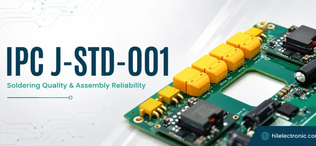
IPC J-STD-001: Classes, Requirements, and RFQ Specification
Figure 1. IPC J-STD-001 image for Highleap Electronics PCB...
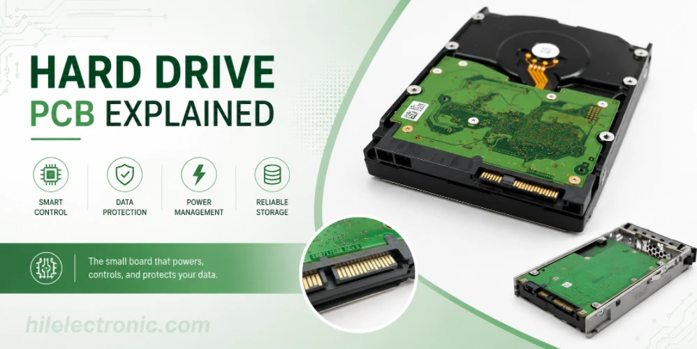
Hard Drive PCB: Function, Failure Modes, and Manufacturing
Figure 1. hard drive PCB image for Highleap Electronics...
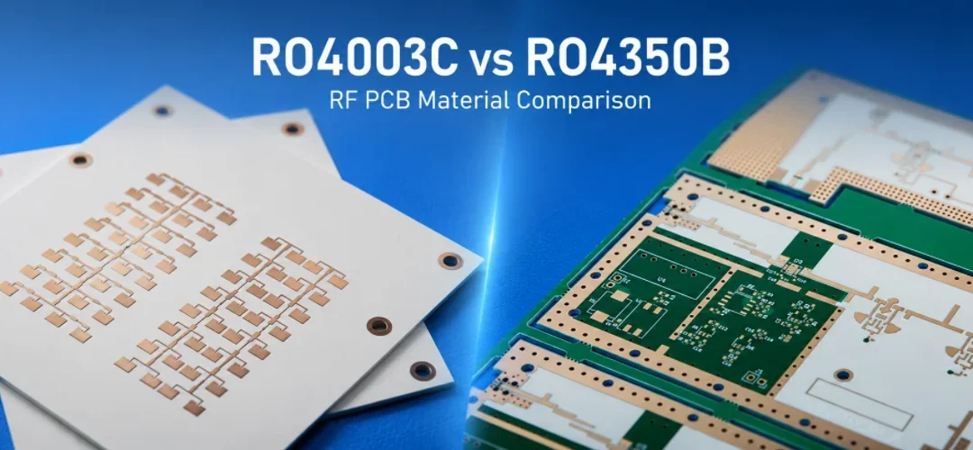
RO4003C vs RO4350B: Rogers Datasheet Values, LoPro Foil, and Stackup Choices
Figure 1. RO4003C vs RO4350B selection depends on...
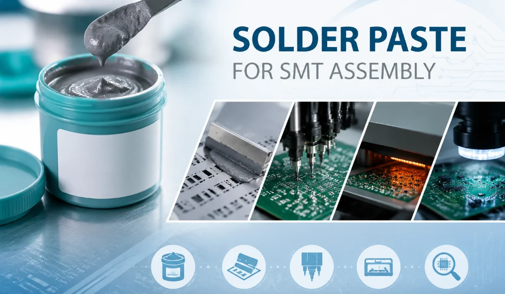
Solder Paste for SMT Assembly: Types, Storage, and Printing Defects
Figure 1. Solder paste selection affects SMT print...
How to get a quote for PCBs
Let us run DFM/DFA analysis for you and get back to you with a report.
You can upload your files securely through our website.
We require the following information in order to give you a quote:
-
- Gerber, ODB++, or .pcb, spec.
- BOM list if you require assembly
- Quantity
- Turn time
In addition to PCB manufacturing, we offer a comprehensive range of electronic services, including PCB design, PCBA (Printed Circuit Board Assembly), and turnkey solutions. Whether you need help with prototyping, design verification, component sourcing, or mass production, we provide end-to-end support to ensure your project’s success. For PCBA services, please provide your BOM (Bill of Materials) and any specific assembly instructions. We also offer DFM/DFA analysis to optimize your designs for manufacturability and assembly, ensuring a smooth production process.