
High-Frequency Aluminum PCB | Balancing Thermal Management and Signal Integrity in RF Applications

Introduction to High-Frequency Aluminum PCB Design
Designing a high-frequency aluminum PCB demands a precise balance between thermal and electrical performance to ensure signal integrity in RF and high-speed systems. As wireless communication and radar technologies move to higher frequencies, designers increasingly seek substrates that combine efficient heat dissipation with stable dielectric characteristics.
Aluminum offers excellent thermal conductivity and mechanical strength but introduces challenges for signal control due to its conductive base. Effective high-frequency aluminum PCB design therefore depends on optimizing the dielectric layer to manage electromagnetic field distribution and impedance consistency. This article explores key design factors that allow aluminum substrates to perform reliably in RF power amplifiers, communication base stations, and high-frequency power conversion systems.
Understanding High-Frequency Aluminum PCB Substrates
High-frequency aluminum PCBs differ from standard metal-core boards mainly in their dielectric composition and thickness control. The aluminum base provides heat spreading and mechanical support, while the dielectric layer ensures low signal loss and impedance stability. Common materials include ceramic-filled epoxy or high-performance polyimide engineered for minimal dissipation at microwave frequencies.
Material Characteristics and Performance Parameters
Key substrate parameters influencing RF performance include:
-
Low dielectric loss – Typical loss tangent between 0.005–0.015 at 2.4 GHz, ensuring stable signal transmission.
-
Controlled dielectric constant – Ranges from 3.5–4.5, suitable for impedance-matched microstrip structures.
-
Optimized dielectric thickness – Generally 0.1–0.3 mm, serving as the main variable for impedance control.
-
Adjustable aluminum base thickness – Typically 1.0–3.0 mm, chosen according to heat dissipation demands.
-
High thermal conductivity – Advanced dielectric formulations achieve 2–4 W/m·K, far exceeding standard FR-4 (~0.3 W/m·K).
-
Shortest thermal path – Direct heat flow from copper traces through the dielectric to the aluminum base minimizes junction temperatures.
These characteristics enable aluminum substrates to maintain both thermal stability and signal integrity in RF power and high-frequency electronic applications.
Signal Integrity Challenges in High-Frequency Aluminum PCB
In RF aluminum PCB design, signal integrity issues primarily arise from the metal substrate’s impact on electromagnetic field distribution. The aluminum base acts as a ground plane, creating asymmetric field patterns in microstrip structures that alter impedance behavior compared to conventional RF laminates. Accurate impedance modeling and adjusted trace width calculations are therefore essential to maintain consistent signal performance.
Primary Loss Mechanisms
- Dielectric loss – Main source of signal degradation, typically 0.3–0.8 dB/in at 2.4 GHz, depending on dielectric material.
- Frequency limitation – Losses increase with frequency, making ≤6 GHz a practical upper limit for most aluminum PCB designs.
- Impedance discontinuities – Occur at component pads, vias, and connectors, disrupting the controlled impedance environment.
Crosstalk and Coupling Effects
- Stronger coupling – Thin dielectric layers and close proximity to the metal base heighten capacitive coupling between traces.
- Improved shielding – The aluminum ground plane enhances EMI containment despite tighter coupling.
- Spacing rules – Maintain ≥3× dielectric thickness between traces to reduce crosstalk below –30 dB at operating frequencies.
These factors highlight the importance of precise dielectric control, impedance tuning, and layout discipline when developing reliable high-frequency aluminum PCBs.

Design Considerations for High-Frequency Aluminum PCB
Dielectric Layer Engineering
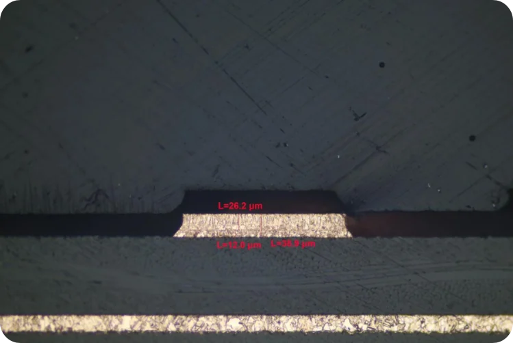
The dielectric layer thickness directly determines characteristic impedance in high-frequency aluminum PCB structures. Thinner dielectrics improve thermal conduction but require narrower trace widths to maintain 50-ohm impedance, which increases copper loss and fabrication difficulty. A balanced range of 0.15 mm to 0.20 mm dielectric thickness typically provides manageable trace widths between 0.3 mm and 0.6 mm for standard designs.
Dielectric constant stability across temperature and frequency affects impedance consistency and phase velocity matching. Materials with low temperature coefficients of dielectric constant minimize impedance drift during operation.
Impedance Control and Stack-up Optimization
Accurate impedance control in high-frequency aluminum PCB design requires electromagnetic simulation during layout development. Standard impedance models must be adjusted to account for the aluminum ground plane and dielectric properties. Tools such as HFSS or Sonnet provide precise field analysis for asymmetric structures.
Stack-up optimization balances electrical and thermal needs through copper weight and dielectric thickness choices. Copper weights of 2 oz or 3 oz reduce resistive loss in high-current paths but complicate impedance matching. Most designs use 1 oz copper with selective plating in high-current regions.
Grounding Architecture
The aluminum base serves as an effective ground plane, providing low-inductance return paths for RF currents. Proper via placement is essential to minimize ground loops while maintaining shielding efficiency. Thermal vias can also function as RF ground connections when placed near sensitive components.
Compartmentalized shielding between circuit sections prevents coupling in mixed-signal designs. Metal shield cans attached to the aluminum base form isolated chambers that enhance electromagnetic compatibility.
Thermal Management Integration
- Shortest thermal path – Direct heat flow from components to the metal base minimizes junction temperatures.
- Strategic via placement – Thermal vias within 2 mm of power devices ensure effective heat transfer.
- CTE compatibility – Copper mesh patterns accommodate thermal expansion differences between layers.
- Interface optimization – Proper thermal interface materials maintain low thermal resistance to external heatsinks.
Surface Finish Selection
Surface finish choice influences both solderability and high-frequency loss. Electroless nickel immersion gold offers excellent planarity and contact resistance but causes slightly higher insertion loss due to nickel’s magnetic properties. For frequencies above 3 GHz, immersion silver or organic solderability preservative finishes reduce skin effect losses while remaining assembly-friendly.
Comparing High-Frequency Aluminum PCB to Alternative Substrates
Understanding material trade-offs guides appropriate substrate selection for specific high-frequency applications. Each material category offers distinct advantages that align with particular performance requirements and cost constraints.
Characteristic
Aluminum PCB
PTFE/Rogers
Ceramic
Characteristic
Aluminum PCB
PTFE/Rogers
Ceramic
Characteristic
Aluminum PCB
PTFE/Rogers
Ceramic
Characteristic
Aluminum PCB
PTFE/Rogers
Ceramic
Characteristic
Aluminum PCB
PTFE/Rogers
Ceramic
Characteristic
Aluminum PCB
PTFE/Rogers
Ceramic
Characteristic
Aluminum PCB
PTFE/Rogers
Ceramic
Practical Engineering Guidelines for High-Frequency Aluminum PCB
Design Verification Approach
Balancing copper thickness and dielectric properties requires iterative optimization during the design phase. Electromagnetic simulation should incorporate actual material properties provided by the PCB fabricator rather than generic database values. This approach accounts for manufacturing process variations that affect final electrical performance. S-parameter extraction from simulation models enables pre-layout verification of critical RF signal paths.
Prototype Validation Methods
Essential validation steps for high-frequency aluminum PCB projects include:
- S-parameter measurements – Vector network analysis characterizes insertion loss, return loss, and impedance matching across the frequency range.
- Thermal imaging – Infrared cameras identify hot spots during powered operation and validate thermal models.
- Time-domain reflectometry – TDR testing locates impedance discontinuities in transmission line structures.
- Power handling tests – Stress testing under maximum rated conditions verifies thermal and electrical margins.
Manufacturing Design Rules
Manufacturing design rules specific to aluminum PCB processes must be incorporated early in layout development. Minimum dielectric thickness tolerances, maximum trace width-to-spacing ratios, and via formation limitations differ from standard rigid PCB capabilities. Early engagement with fabrication partners prevents costly redesign cycles and ensures first-pass success.

Applications of High-Frequency Aluminum PCB Technology
RF Power Amplifiers
RF power amplifier modules for cellular base stations represent the largest application segment for high-frequency aluminum PCB technology. These designs typically operate between 700 MHz and 3.5 GHz with output power levels from 10 watts to over 100 watts per channel. The aluminum substrate efficiently removes heat from GaN or LDMOS transistor dies while the dielectric layer maintains controlled 50-ohm matching networks.
Automotive Radar Systems
LED radar modules for automotive and industrial applications increasingly adopt aluminum PCB constructions that combine RF circuitry with high-intensity illumination. The aluminum base serves both as heatsink for LED arrays and ground plane for millimeter-wave radar transceivers operating at 24 GHz or 77 GHz. This integration reduces system size and cost while improving thermal reliability.
Communication Infrastructure
Communication infrastructure power amplifiers for distributed antenna systems leverage aluminum PCB thermal advantages in compact form factors. These modules must deliver consistent RF performance across wide temperature ranges while maintaining reliability in outdoor installations. High-frequency aluminum PCB designs enable cost-effective solutions that meet both electrical specifications and environmental requirements.
High-Frequency Power Conversion
High-frequency DC-DC converters operating at switching frequencies above 1 MHz benefit from aluminum substrate thermal management combined with controlled impedance power delivery networks. The conductive base provides stable ground reference for high di/dt current paths while efficiently removing heat from power semiconductors.
Conclusion
Successful high-frequency aluminum PCB design demands integrated consideration of thermal, electrical, and mechanical requirements throughout the development process. Impedance control depends on precise dielectric layer specification and electromagnetic simulation validation. Signal integrity preservation requires attention to loss mechanisms, discontinuity management, and proper grounding implementation. The material selection decision should align with specific application requirements, with aluminum PCB technology delivering optimal value in power RF applications where thermal management justifies modest increases in dielectric loss.
Highleap Electronics High-Frequency Aluminum PCB Capabilities
Highleap Electronics provides comprehensive manufacturing support for complex high-frequency aluminum PCB projects:
- Advanced material selection – Access to specialized dielectric formulations optimized for RF performance and thermal conductivity.
- Precision impedance control – Controlled dielectric thickness tolerances within ±10% for consistent 50-ohm and 75-ohm transmission lines.
- Thermal via optimization – Strategic placement and formation of thermal vias for maximum heat transfer efficiency.
- RF testing services – In-house S-parameter measurement and impedance verification for production validation.
- Design consultation – Technical support during layout phase to optimize stack-up configurations and manufacturing feasibility.
For complex RF aluminum PCB designs requiring both electrical precision and thermal reliability, contact Highleap Electronics to discuss your project specifications and leverage our proven manufacturing processes.

Recommended Posts
Prepreg Material for Multilayer PCB Manufacturing
On this page Understanding Core and Prepreg Materials...
Low Loss PCB Fabrication for High-Speed Digital and RF Applications
On this page What Is Low Loss PCB Fabrication When Do You...

PCB Laminate Lead Time and Production Scheduling
On this page Why Laminate Lead Times Vary Standard vs...
Low Dk Low Df PCB Material for High Speed Signals
Figure 1. Low loss PCB material selection for high speed...
How to get a quote for PCBs
Let‘s run DFM/DFA analysis for you and get back to you with a report. You can upload your files securely through our website. We require the following information in order to give you a quote:
-
- Gerber, ODB++, or .pcb, spec.
- BOM list if you require assembly
- Quantity
- Turn time
In addition to PCB manufacturing, we offer a comprehensive range of electronic services, including PCB design, PCBA, and turnkey solutions. Whether you need help with prototyping, design verification, component sourcing, or mass production, we provide end-to-end support to ensure your project’s success.
For PCBA services, please provide your BOM (Bill of Materials) and any specific assembly instructions. We also offer DFM/DFA analysis to optimize your designs for manufacturability and assembly, ensuring a smooth production process.