
Schematic Meaning for PCB Design and Manufacturing

In electronics, schematic meaning refers to the logical representation of a circuit using standardized symbols and electrical connections. A schematic shows how components are connected, how signals flow, and how the circuit is intended to work before PCB design and physical implementation begin.
A schematic is not the same as a PCB layout. It explains electrical intent, not real component placement. That is why engineers use it as the starting point for circuit review, debugging, design validation, and later transition into PCB fabrication and PCB assembly.
At Highleap Electronics, we help customers turn circuit concepts into manufacturable products, and a well-prepared schematic diagram is one of the most important starting points in that process. This guide explains schematic meaning in practical engineering terms, how schematics are used, how they differ from related drawings, and why they matter in real PCB development.
Get a Quote for Your PCB Project
Table of Contents
- Schematic Meaning in Electronics
- What Information a Schematic Shows
- Schematic vs Diagram vs PCB Layout
- Why a Schematic Matters in PCB Design
- How Engineers Use Schematics in Real Projects
- Common Mistakes When Reading or Creating Schematics
- From Schematic to PCB Manufacturing and Assembly
- Schematic Meaning FAQ
Schematic Meaning in Electronics
In electronics, a schematic is a symbolic representation of a circuit. It uses standardized symbols to show components such as resistors, capacitors, diodes, transistors, ICs, connectors, switches, and power sources, along with the electrical connections between them.
So when people ask for the schematic meaning, the most accurate answer is this: a schematic is the circuit’s logical map. It explains how the design works electrically, but it does not show the real physical placement of parts on the PCB.
This distinction is important. A schematic answers questions like:
- Which components are connected together?
- What is the function of each block in the circuit?
- Where does power enter and how is it distributed?
- How do signals move from one stage to another?
- What is the electrical intention of the design?
In other words, the schematic describes the circuit’s logic, not its physical shape.
What Information a Schematic Shows
A well-made schematic contains much more than symbols and lines. It is a structured engineering document that communicates how a circuit is supposed to function and how it should be interpreted by designers, reviewers, layout engineers, test engineers, and manufacturing teams.
A typical electronic schematic may include:
- Component symbols: resistors, capacitors, inductors, diodes, transistors, ICs, relays, connectors, sensors, and other parts
- Reference designators: labels such as R1, C5, U2, J1, or D3 that identify each component uniquely
- Net connections: the electrical paths between component pins
- Power rails: such as 3.3V, 5V, 12V, GND, VCC, VBAT, and others
- Signal names: labels that help identify buses, clocks, control signals, analog lines, or communication nets
- Functional blocks: logical sections such as power supply, MCU, communication interface, sensor front-end, or driver stage
- Notes and design intent: comments, values, tolerances, part descriptions, or circuit behavior details
This is why the schematic is often the first document engineers use when they want to understand a design quickly. It gives the electrical story of the product before physical implementation begins.
Schematic vs Diagram vs PCB Layout
One of the most common sources of confusion is the difference between a schematic, a general diagram, and a PCB layout. These terms are related, but they do not mean the same thing.
| Term | Main Purpose | What It Shows |
|---|---|---|
| Schematic | Electrical logic | How components are electrically connected |
| Diagram | General explanation | A visual representation of a system, concept, or process |
| PCB layout | Physical implementation | Real part placement, routing, copper, pads, vias, and board outline |
A schematic may look abstract, but that is because it is not trying to represent physical placement. For example, two connected components may be placed far apart in the actual PCB layout, even though they appear close together in the schematic. The schematic is optimized for readability of electrical function, while the PCB layout is optimized for manufacturability, signal integrity, thermal behavior, and mechanical fit.
Why a Schematic Matters in PCB Design
In PCB development, the schematic is the starting point for almost everything that follows. It defines the electrical intent of the board and becomes the source for netlists, part mapping, PCB layout constraints, test strategy, and design review.
A correct schematic helps ensure:
- Electrical functionality: the circuit performs as intended
- Correct component selection: the right values and part types are assigned
- Reliable PCB layout: nets, pin assignments, and functional grouping are correct before layout begins
- Easier debugging: engineers can trace faults and signal paths more effectively
- Clear communication: all stakeholders can understand the design logic
If the schematic contains pin errors, missing decoupling, wrong power connections, bad grounding strategy, or unclear net naming, those problems usually carry forward into the PCB. That is why strong schematic review is just as important as strong PCB layout review.

How Engineers Use Schematics in Real Projects
In actual engineering work, a schematic is used throughout the full product development cycle, not just at the beginning.
Engineers use schematics to:
- Design new circuits: define the structure and behavior of the system
- Review design logic: check power flow, signal paths, interfaces, and protection circuits
- Create PCB layouts: transfer the electrical design into the physical board environment
- Support firmware work: help embedded engineers understand pin mapping, interfaces, and hardware dependencies
- Troubleshoot failures: identify likely fault locations and understand system behavior
- Prepare for manufacturing: confirm design intent before fabrication and assembly
For complex electronics, the schematic is often the most efficient way to understand the architecture of the product. A good engineer can read a schematic and quickly see where power enters, how the MCU is connected, what interfaces are present, and where the most sensitive parts of the design are located logically.
Common Mistakes When Reading or Creating Schematics
Not all schematics are equally useful. A schematic can be technically correct and still be hard to read, hard to review, or easy to misunderstand. That is why clarity matters as much as correctness.
Common schematic problems include:
- Poor net naming: unclear or inconsistent signal names make debugging harder
- Missing power detail: hidden rails or incomplete supply connections create confusion
- Messy organization: unrelated blocks mixed together reduce readability
- Unclear symbol choice: symbols that do not match convention slow down understanding
- Missing component values or notes: makes review and BOM preparation more difficult
- Incorrect pin mapping: one of the most dangerous errors because it can propagate directly into PCB layout
A strong schematic should be both electrically correct and easy for another engineer to review. In professional electronics development, readability is part of quality.
From Schematic to PCB Manufacturing and Assembly
Although a schematic itself is not used directly to fabricate a PCB, it strongly influences whether the design can move smoothly into manufacturing and assembly. The schematic defines the electrical structure that later becomes the PCB layout, component list, and manufacturing package.
For a PCB manufacturing and assembly company like Highleap Electronics, the schematic matters because it affects:
- BOM accuracy: whether parts are properly defined and manufacturable
- Layout quality: whether electrical intent has been transferred correctly into the board design
- Assembly readiness: whether footprints, polarity, and package logic are correct
- Testing strategy: whether the board can be inspected and functionally verified
- Engineering review: whether potential design issues can be identified before production
In short, the schematic is one of the earliest documents that determines whether the final PCB project will move cleanly from design into fabrication and assembly. A strong schematic helps reduce later risk, rework, and production delays.
Schematic Meaning FAQ
What does schematic mean in electronics?
In electronics, schematic means a symbolic drawing that shows how components are electrically connected in a circuit. It represents function and logic, not physical layout.
Is a schematic the same as a circuit diagram?
In many cases, people use the terms interchangeably. However, schematic usually refers more specifically to the formal symbolic representation of an electrical circuit.
Does a schematic show the physical PCB layout?
No. A schematic shows electrical connections and design logic. The PCB layout shows the actual physical placement of parts and copper routing on the board.
Why is a schematic important before PCB manufacturing?
Because it defines the circuit’s electrical intent. Errors in the schematic often lead to errors in layout, assembly, testing, and final product performance.
Who uses schematics in a real electronics project?
Hardware engineers, PCB layout designers, firmware engineers, test engineers, manufacturing engineers, and troubleshooting teams all use schematics at different stages of development.
To move from schematic to a real product efficiently, many teams validate the design first with a prototype PCB before releasing it to full production.

Recommended Posts
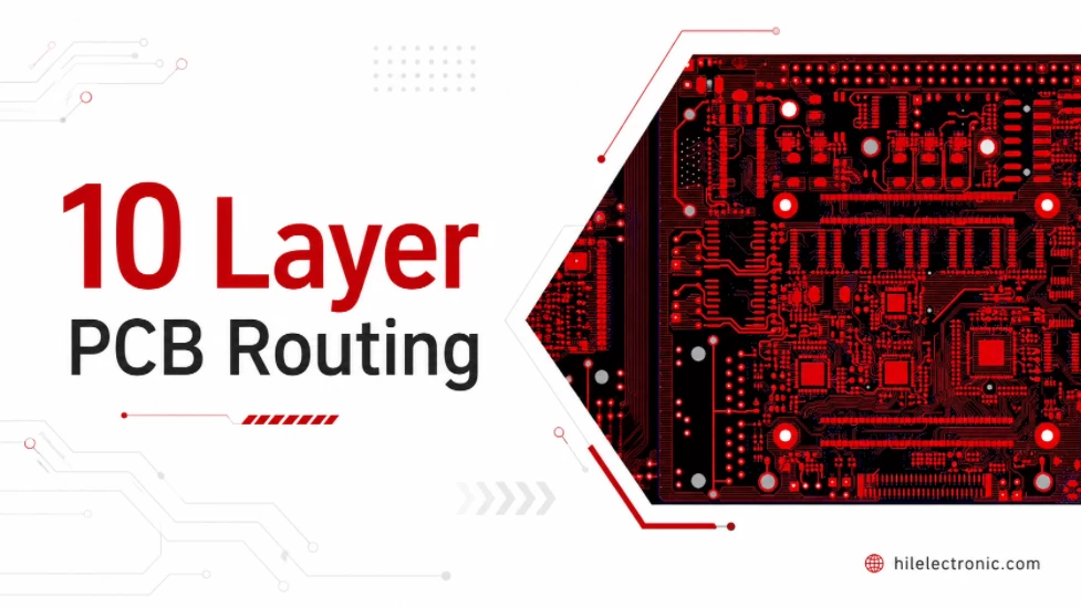
10 Layer PCB Routing Rules for DDR5, PCIe and Crosstalk
Figure 1. 10 layer PCB routing rules for DDR5 PCIe and...
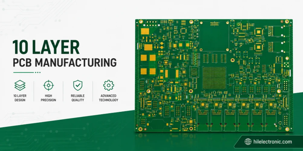
10 Layer PCB Manufacturer for Rigid, Flex and Rigid-Flex
Figure 1. 10 layer PCB manufacturer production capability....
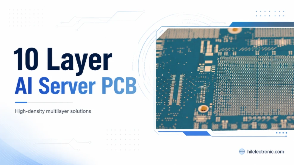
10 Layer AI Server PCB Engineering for Accelerator Hardware
Figure 1. 10 layer AI server PCB for accelerator hardware....
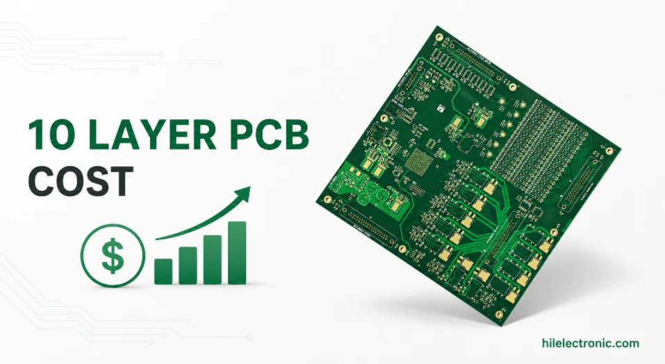
10 Layer PCB Cost Drivers for Materials, HDI and Testing
Figure 1. 10 layer PCB cost drivers for materials HDI and...
How to get a quote for PCBs
Let us run DFM/DFA analysis for you and get back to you with a report.
You can upload your files securely through our website.
We require the following information in order to give you a quote:
-
- Gerber, ODB++, or .pcb, spec.
- BOM list if you require assembly
- Quantity
- Turn time
In addition to PCB manufacturing, we offer a comprehensive range of electronic services, including PCB design, PCBA (Printed Circuit Board Assembly), and turnkey solutions. Whether you need help with prototyping, design verification, component sourcing, or mass production, we provide end-to-end support to ensure your project’s success. For PCBA services, please provide your BOM (Bill of Materials) and any specific assembly instructions. We also offer DFM/DFA analysis to optimize your designs for manufacturability and assembly, ensuring a smooth production process.