
Quick Turn Rogers RO4360G2 PCB Prototype for 5G Design

Rogers RO4360G2 was formulated specifically to eliminate this compromise. As a hydrocarbon ceramic-filled thermoset laminate, it delivers an unusually high Dielectric Constant (Dk of 6.15) but processes identically to standard FR-4. For teams looking to build a reliable custom Rogers RO4360G2 5G PCB, this material provides the electrical stability of a high-frequency printed circuit board without the severe lead-time bottlenecks associated with traditional PTFE processing.
Request a RO4360G2 Engineering Quote
Table of Contents
Why Choose Dk 6.15 for 5G Miniaturization?
In radio frequency design, the physical size of a resonant circuit (like a patch antenna array or power divider) is inversely proportional to the square root of the substrate’s dielectric constant.
By shifting from a standard Dk 3.5 RF material to RO4360G2’s Dk of 6.15, hardware engineers can shrink the physical dimensions of their RF structures by approximately 20% to 30%. This space compression is absolutely critical for densely packed active antenna units (AAUs). Furthermore, the material maintains a very low Dissipation Factor (Df = 0.0038 at 10 GHz), ensuring that the tightly routed signal paths do not suffer from severe insertion loss.
Core Thermomechanical Specifications
Electrical performance means nothing if the board fails during soldering or field deployment. RO4360G2 is heavily filled with ceramic, granting it remarkable dimensional stability compared to standard woven-glass laminates.
| Key Parameter | Value (Typical) | Manufacturing & Application Impact |
|---|---|---|
| Dielectric Constant (Dk) | 6.15 ± 0.15 | Reduces physical footprint; requires highly precise trace etching to hit 50-ohm impedance targets. |
| Dissipation Factor (Df) | 0.0038 @ 10 GHz | Low insertion loss, preserving signal integrity for power amplifiers and transceivers. |
| Z-Axis CTE | 28 ppm/°C | Matches copper expansion; ensures excellent Plated Through-Hole (PTH) reliability during reflow. |
| Thermal Conductivity | 0.81 W/m/K | Aids in effectively dissipating heat from active RF surface-mount components. |
Deep Dive: Bypassing Plasma Desmear in Fabrication
If you ask any CAM engineer what slows down microwave board production, the answer is “PTFE via preparation.” When a CNC drill bit cuts through Teflon, the frictional heat causes the material to smear across the inner copper layers. Removing this smear requires extremely toxic sodium etchants or bottlenecking the production line by putting the panels into a vacuum plasma chamber.
Because RO4360G2 is a glass-reinforced hydrocarbon thermoset, it does not melt and smear like PTFE.
A proficient high-speed Rogers RO4360G2 PCB factory can drill, desmear, and plate these boards using the exact same standard chemistry lines used for standard FR-4. This “FR-4 processability” is the material’s greatest hidden asset. It drastically cuts down manufacturing lead times and directly lowers the overall Rogers RO4360G2 PCB prototype price, allowing R&D teams to iterate faster while maintaining strict RF tolerances.
Impedance Control Reality
While hole preparation is easy, RF etching is unforgiving. A Dk of 6.15 means traces must be exceptionally narrow. A 1-mil over-etch error on a Dk 6.15 material will cause a much more severe impedance mismatch than on a standard Dk 3.5 board. Vacuum etching lines and Laser Direct Imaging (LDI) are mandatory to keep trace sidewalls perfectly vertical.
Controlling Warpage in Hybrid RF Stackups
To optimize project budgets, it is extremely rare to use RO4360G2 for all layers of a complex telecommunications board. Instead, designers create hybrid stackups—placing the Rogers material on layers 1 and 2 for the microwave routing, while utilizing lower-cost High-Tg FR-4 (like Isola 370HR) for the internal power, ground, and digital logic layers.
However, co-curing a ceramic-filled hydrocarbon with an epoxy FR-4 introduces a massive mechanical risk: Asymmetric Warpage (The Potato-Chip Effect).
Different resin systems have different Glass Transition Temperatures (Tg) and melt viscosities. If the press cycle ramps up too fast, the FR-4 prepreg might flow while the Rogers prepreg remains stiff. When the board cools down, the differing thermal contraction rates will cause the panel to bow aggressively. As an experienced China Rogers RO4360G2 PCB manufacturer, Highleap Electronics prevents this by utilizing asymmetric press padding and heavily customized thermal ramp recipes, ensuring the multilayer bare board fabrication results in perfectly flat panels ready for assembly.
Partnering with a Turnkey RO4360G2 Supplier
Achieving a reliable sub-6 GHz or mmWave product is a two-step process: precision fabrication followed by flawless component mounting. Any solder voids underneath a high-power RF amplifier pad can detune the circuit and cause catastrophic overheating.
We highly recommend keeping both phases under one roof to prevent supplier miscommunication. When searching for a Rogers RO4360G2 low loss PCB supplier, ensure they have the capability to validate both the bare board and the final solder joints. At Highleap Electronics, our comprehensive Rogers RO4360G2 PCB fabrication service integrates seamlessly with our advanced PCBA manufacturing lines. We utilize 3D X-Ray (AXI) inspection to guarantee void-free thermal grounding and exact RF component placement.
Whether you need a rapid prototype for a new phased array or volume production for 5G infrastructure, our engineering team is ready to review your Gerber files and stackup requirements.

Recommended Posts
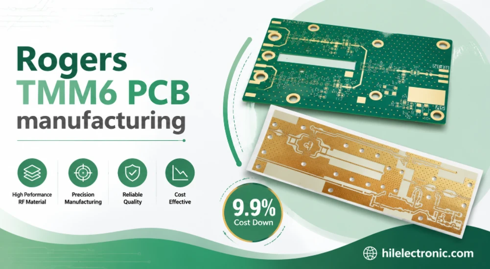
Rogers TMM6 PCB Manufacturing for Microwave Filters
Table of contentsWhy Microwave Filter Designers Use...
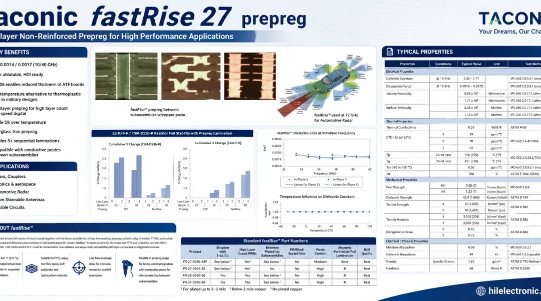
Taconic fastRise 27 Prepreg PCB Bonding and HDI Fabrication Service
Table of contentsWhat fastRise 27 Is—and What You Are...
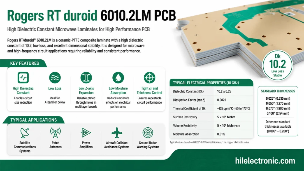
Rogers RT/duroid 6010.2LM PCB Manufacturer and Fabrication Service
Table of contentsIs RT/duroid 6010.2LM the Right Material...
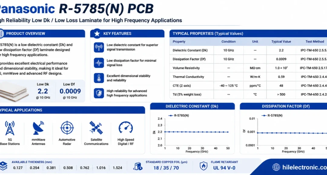
Panasonic R-5785(N) MEGTRON 7 PCB Manufacturer and Fabrication
Table of contentsWhen a Design Should Move to R-5785(N) /...
How to get a quote for PCBs
Let us run DFM/DFA analysis for you and get back to you with a report.
You can upload your files securely through our website.
We require the following information in order to give you a quote:
-
- Gerber, ODB++, or .pcb, spec.
- BOM list if you require assembly
- Quantity
- Turn time