
Circuit Board Layout: Expert Techniques to Avoid Pitfalls

Designing an effective circuit board layout goes beyond following standard guidelines; it requires nuanced decisions to sidestep common traps that can jeopardize performance, reliability, and manufacturability. In this article, we’ll focus on advanced, often-overlooked techniques and insights that can help PCB designers avoid frequent pitfalls and create optimized layouts for even the most demanding applications.
1. Precision in Signal Return Path Planning
One common mistake, even among seasoned designers, is underestimating the importance of clear, low-impedance return paths for high-speed signals. A poor return path can lead to EMI issues, increased signal degradation, and unpredictable behavior.
-
Ground Plane Segmentation: Avoid segmenting ground planes in critical areas. Designers sometimes route signals over a segmented ground plane, causing return currents to take longer paths, which can induce noise. Ensure all high-speed signals have a continuous return path to minimize these effects.
-
Stitching Capacitors: When crossing from one ground plane to another, such as from a digital to an analog ground plane, use stitching capacitors to provide a short path for high-frequency return currents. This reduces potential for noise coupling and maintains signal integrity across boundaries.
2. Adaptive Power Decoupling Strategies
Decoupling capacitors are not just a matter of placing standard values close to ICs. Choosing the right values and placements based on specific requirements can make a significant difference.
-
Custom Decoupling Networks: For high-current applications, use a mix of capacitor values to cover a broad frequency range. Capacitors in the 10-100 nF range address high frequencies, while larger capacitors handle lower frequencies. Avoid overloading with capacitors at a single frequency range, as this can lead to resonant peaks that cause power instability.
-
Capacitor Placement Priority: While general advice suggests placing capacitors close to power pins, prioritize placement for ICs with critical power demands, such as FPGAs or processors, where insufficient decoupling could impact performance. Less critical ICs can share decoupling resources to save space and reduce unnecessary complexity.
3. Avoiding Thermal Expansion Mismatch in Multi-Layer Boards
When dealing with multi-layer boards that combine materials with differing thermal expansion rates, such as FR4 with copper-heavy layers, thermal mismatch can cause stress and warping, especially in high-power designs.
-
Balanced Layer Stack-Up: Ensure symmetrical copper distribution on each layer to prevent warping. Unbalanced copper weight can lead to bowing during manufacturing. To avoid this, mirror dense copper areas on opposite layers or add dummy copper fills for balance.
-
Expansion-Compensating Materials: For designs that undergo extreme temperature cycles, consider high-performance laminates with matched thermal expansion rates. These materials can improve longevity and reduce the risk of layer separation in mission-critical applications, such as aerospace and automotive electronics.

PCB Circuit Board Layout
4. Strategic Via Management: Techniques to Avoid Signal and Power Issues in PCB Design
Vias are indispensable in circuit board design, especially for complex multi-layer boards where they serve as the connections between different layers. However, if not managed strategically, vias can lead to signal integrity issues, power inefficiencies, and thermal problems that affect the board’s overall performance. Understanding how to optimize via usage can not only improve signal performance and thermal management but also help reduce costs. Below, we dive into best practices, tips, and cost-saving strategies for managing vias effectively.
Choosing the Right Type of Via for the Design
Vias come in several forms—through-hole, blind, buried, and microvias—each with distinct uses and implications for design complexity, cost, and performance.
- Through-Hole Vias: The most common type, through-hole vias, span the entire PCB thickness and are suitable for lower-density boards. However, they create stubs on high-speed signals, which can degrade signal integrity. Back-drilling can remove these stubs, though it adds manufacturing cost.
- Blind and Buried Vias: Blind vias connect the surface to an internal layer, while buried vias connect two internal layers without reaching the surface. Both help save space, but are costlier to manufacture. Use them sparingly in dense designs or high-speed circuits where reducing via stub length and minimizing signal interference is critical.
- Microvias: Typically used in High-Density Interconnect (HDI) boards, microvias have smaller diameters and can only span one layer. They’re ideal for fine-pitch designs and can reduce board thickness, but they are significantly more expensive. Use microvias selectively in areas requiring high-speed interconnects or compact component placement.
When budget allows only limited blind or buried vias, reserve them for areas with the highest signal integrity needs, such as high-speed differential pairs. For less critical connections, standard through-hole vias are more economical.
Anti-Pad Optimization for High-Frequency Signals
High-frequency signals face particular challenges when routed through vias, as they can experience impedance mismatches that lead to reflections and signal loss. The anti-pad, or the void around the via in the ground plane, plays a crucial role in determining the via’s capacitance.
- Controlling Anti-Pad Size: Adjusting the anti-pad size can help balance the capacitance and inductance of the via. A larger anti-pad reduces capacitance, minimizing the signal degradation. However, this can also increase inductance, so finding the right balance is key. For most high-frequency designs, using simulation tools to fine-tune anti-pad size for specific signal speeds is essential.
- Using Grounded Stitching Vias: For signals that are especially sensitive to noise, such as RF or high-speed digital lines, consider placing stitching vias around the primary signal via. These stitching vias are connected to ground and help create a local ground shield, reducing potential EMI and crosstalk.
Use 3D electromagnetic simulation tools to model via structures in critical high-speed areas, optimizing anti-pad size and placement for each specific design rather than relying on standard sizes.
While optimizing anti-pad sizes for every via is ideal, focus on critical signal paths like clock lines or data buses. Using standard via structures on non-critical paths reduces design complexity and manufacturing costs.
Thermal Via Arrays for Effective Heat Dissipation
Thermal management is crucial, especially in high-power designs where components like power regulators, MOSFETs, and LEDs can generate significant heat. Thermal vias are small vias that help transfer heat from the top layer to inner layers or even the bottom layer, aiding in dissipation.
- Creating Thermal Via Arrays: Instead of one large via, an array of smaller vias can enhance thermal transfer due to increased surface area contact. Position thermal vias under heat-generating components and connect them to large copper pours on inner layers or the bottom layer, creating a direct path for heat to dissipate.
- Via Fill Options: For vias under components that require a stable thermal connection, consider filled or plugged vias. Filled vias improve heat conduction and provide mechanical stability, which is essential under components like power transistors. Note that filling vias increases cost, so this should be used selectively for high-power areas.
- Copper Pour and Plane Connection: Connect thermal vias to a dedicated ground or power plane that acts as a heat spreader. Increasing copper thickness (e.g., 2 oz instead of 1 oz) on layers with thermal vias can further enhance heat dissipation but increases board cost. Evaluate cost versus thermal performance requirements when selecting copper thickness.
Space thermal vias in an array with a typical center-to-center spacing of 1.0 to 1.5 mm to balance thermal performance and structural integrity. Also, avoid excessive via density as it can complicate manufacturing and increase costs.
Use standard-sized thermal vias and avoid over-specifying via density unless necessary. For designs with moderate heat requirements, a sparse via pattern may be sufficient, reducing the need for costly thermal vias.
Minimizing Signal Delay and Power Loss with Via Placement
Signal delay and power loss can become issues in designs where vias are overused or placed without a clear strategy. The placement and type of vias used in power and ground planes can significantly impact performance, especially in high-current or high-speed designs.
- Parallel Vias for High Current Paths: High-current paths, such as power supply lines, should not rely on a single via. Instead, use multiple vias in parallel to share the current load and reduce resistance. This prevents localized heating and potential reliability issues over time.
- Avoiding Unnecessary Layer Transitions: Each via introduces a small amount of inductance, which can accumulate and cause signal delay. Minimize layer transitions for high-speed signals by planning trace routing effectively. For high-speed buses, keep layer changes to an absolute minimum, as each via can add delay and signal degradation.
- Ensuring Short Return Paths: For signals that change layers, ensure that return paths are as close as possible to minimize loop areas. For example, if a signal via moves from layer 1 to layer 3, place a ground via nearby to provide a low-impedance return path, reducing noise and EMI.
In power distribution networks (PDNs), distribute vias uniformly along the path rather than concentrating them in one spot. This enhances current distribution and prevents bottlenecks that lead to voltage drops.
Instead of using a dense via array on every power line, evaluate the current requirements. For low-current lines, fewer vias can suffice, reducing both manufacturing complexity and cost.
Advanced Techniques: Staggered Microvias and Back-Drilling
For extremely high-density or high-frequency designs, advanced via techniques like staggered microvias and back-drilling can optimize performance, though they come with added complexity and cost considerations.
- Staggered Microvias: For HDI boards, staggered microvias (placing vias at staggered positions instead of stacking) improve reliability and can be cost-effective compared to stacked vias. Staggering also reduces mechanical stress during manufacturing, which is critical in designs with multiple microvia layers.
- Back-Drilling to Minimize Stubs: Via stubs are the portions of vias that do not connect to a signal layer, and they act as unwanted antennas in high-speed designs. Back-drilling removes these stubs, reducing reflections and improving signal integrity. However, back-drilling requires precision and adds manufacturing costs, so it should be reserved for critical high-speed signal paths.
Use staggered microvias instead of stacked vias when possible, as they typically require fewer manufacturing steps. For back-drilling, limit its use to essential signal lines to avoid excessive production costs.
5. Managing Crosstalk Beyond the Basics
Simply spacing traces apart is not always enough to mitigate crosstalk, especially as frequencies rise and board real estate becomes more limited.
-
Perpendicular Routing Across Layers: When routing across multiple layers, route critical signals perpendicular to each other on adjacent layers to reduce capacitive coupling. For instance, if a signal runs horizontally on layer 1, it should ideally run vertically on layer 2.
-
Guard Traces for High-Speed Signals: While guard traces are commonly used, they’re not effective without proper grounding. Always connect guard traces to a solid ground plane using vias at both ends and along the trace to create an effective shield for high-speed signals.
6. Advanced Impedance Control for Mixed-Signal Designs in Circuit Board Layout
In circuit board layout for mixed-signal designs, where analog and digital signals coexist, managing impedance control is essential to ensure signal integrity. The varied impedance requirements of digital and analog signals make it challenging to prevent crosstalk, noise, and signal reflections. Understanding and managing different impedance types can help designers minimize interference between analog and digital domains and maintain signal clarity.
Types of Impedance in Mixed-Signal Circuit Board Layout
- Characteristic Impedance
Characteristic impedance is the inherent impedance of a transmission line, determined by its physical dimensions and the properties of the surrounding materials. In PCB design, maintaining characteristic impedance is crucial for high-speed signals to prevent signal reflections. Typical values are 50 ohms for single-ended traces and 100 ohms for differential pairs. Consistent characteristic impedance along traces helps to ensure signal integrity, particularly in digital signals and high-frequency applications. - Differential Impedance
Differential impedance is specific to paired signals, such as those used in USB, HDMI, or Ethernet, where signals are sent across two conductors. It is the impedance measured between the two conductors as a pair, typically around 100 to 120 ohms. Properly controlled differential impedance ensures minimal signal skew and maintains synchronization between the two signals, essential for high-speed data integrity. - Single-Ended Impedance
Single-ended impedance applies to traces where a signal travels on a single conductor with respect to a ground reference. This is common in analog circuits and slower digital signals. Single-ended impedance typically targets around 50 ohms, and maintaining this impedance is essential to reduce signal loss and reflections for clearer, more reliable signal transmission. - Common Mode Impedance
Common mode impedance represents the impedance seen by the common-mode signal between two conductors relative to ground. In mixed-signal designs, this type is especially relevant when managing electromagnetic interference (EMI) and noise coupling. High common-mode impedance helps reduce noise in sensitive analog circuits by suppressing unwanted common-mode signals. - Controlled Impedance
Controlled impedance refers to the deliberate design and management of characteristic, differential, and single-ended impedances. It is essential for high-frequency circuits, as even small impedance mismatches can lead to signal reflections and loss. Controlled impedance is achieved through precise trace width, spacing, and layer stack-up adjustments, typically verified with simulation tools. - Impedance Matching
Impedance matching involves adjusting the load impedance to match the source impedance, minimizing reflections at the interface between components or circuits. This concept is particularly significant in RF and high-speed digital designs, where impedance mismatches can degrade performance. By matching impedances, designers can ensure maximum power transfer and minimal signal loss.
Dedicated Ground Planes with Tight Coupling
To prevent high-frequency digital noise from affecting sensitive analog signals, digital and analog ground planes are often separated in mixed-signal circuit board layouts. However, these planes must be managed carefully to prevent issues like ground loops and impedance discontinuities.
- Separate but Coupled Ground Planes: Ideally, place digital and analog ground planes close to each other with tight coupling to control noise without causing impedance mismatches. This design minimizes ground loop potential while offering efficient return paths. Use stitching capacitors across the boundaries to ensure continuity for high-frequency signals.
- Single Unified Ground Plane with Isolation: In low-noise applications, a single ground plane may work if isolated sections are created to shield analog components from digital noise. This approach can simplify design and save space, but requires thorough simulation to confirm effective impedance matching and noise isolation.
- Simulation for Impedance Matching: Use electromagnetic (EM) simulation tools to analyze ground plane behavior, particularly how closely-coupled planes interact and impact signal integrity. Simulating the layout helps detect potential impedance mismatches and allows for adjustments before production.
Stub Minimization in Differential Pairs
Differential pairs, commonly used for high-speed data transmission, are particularly sensitive to impedance mismatches, which can lead to signal degradation. Via stubs, or the unused sections of vias, can create impedance discontinuities that are detrimental to differential signals.
- Back-Drilling to Remove Stubs: Via stubs act as antennas, introducing unwanted reflections that interfere with differential signal integrity. Use back-drilling to remove the excess via material, especially for data rates above 5 Gbps. This reduces impedance mismatches, maintaining signal clarity and minimizing noise in high-speed connections.
- Optimized Routing for Differential Pairs: In mixed-signal designs, it’s essential to maintain consistent spacing and controlled impedance along differential pairs. Minimize layer changes to reduce the need for additional vias, as each transition introduces potential stubs. When layer changes are necessary, controlled-depth drilling can help to reduce stub lengths without requiring full back-drilling.
Additional Best Practices for Impedance Control in Mixed-Signal Circuit Board Layouts
- Avoid Overlapping Power and Ground Planes: Placing digital power planes directly over analog ground planes can create coupling capacitance, allowing noise to propagate into analog sections. Keep these planes separated vertically and horizontally to prevent unintended coupling in sensitive analog areas.
- Use Guard Traces and Shielding Techniques: Place grounded guard traces or shields around critical analog components to further isolate them from digital noise. In high-noise environments, adding copper pours connected to ground around analog traces provides additional protection against EMI and crosstalk.
- Integrated Impedance Control in Stacked Vias: For designs with high-density components requiring stacked vias, maintain impedance continuity by optimizing the anti-pad size around each via to prevent capacitive loading. This technique is especially valuable for boards requiring compact layouts without compromising signal integrity.
Managing impedance effectively in mixed-signal circuit board layouts is essential for achieving robust signal integrity and reducing interference between analog and digital domains. By implementing techniques such as tightly coupled ground planes, back-drilling to minimize stubs, and optimizing routing for differential pairs, designers can enhance the performance of their mixed-signal PCBs. With careful impedance control, you can create high-quality boards that meet rigorous performance standards, ensuring reliable operation across a range of complex applications. As a PCB & PCBA manufacturer, we offer the expertise and precision needed to achieve these advanced impedance control strategies, helping you bring your mixed-signal designs to market with confidence.
7. DFM Considerations: Proactively Addressing Manufacturability Issues
Designers often overlook manufacturability until late in the design process, leading to production delays and costly reworks.
-
Avoiding Overly Tight Tolerances: PCB manufacturers may struggle with fine trace and space tolerances. Avoid pushing the limits unless necessary, and consult with your manufacturer to understand their capabilities. Relaxing tolerances can improve yield and reduce costs without compromising performance in many designs.
-
Avoiding Sharp Corners: Sharp internal corners on pads or cutouts can lead to stress concentration, risking board failure over time. Use rounded corners, especially on cutouts and large copper areas, to enhance mechanical durability and avoid manufacturing issues.
8. Simulation and Testing: Leveraging Pre-Production Verification Tools
The importance of simulation is often underestimated, but thorough pre-production testing can prevent most issues from becoming field failures.
-
Power Integrity Simulation: Beyond basic decoupling capacitor placement, simulate the entire power distribution network (PDN) to identify hotspots, excessive voltage drops, or resonance issues. Tools like PowerSI can provide insights on how current flows across planes, highlighting weak spots before physical prototyping.
-
Thermal and Stress Simulation for Reliability: In high-density or high-power designs, thermal stress can accumulate over time, affecting board reliability. Tools like Ansys SIwave or Altium’s thermal simulation can model heat distribution across layers, allowing you to adjust layouts to mitigate thermal hotspots or warping risks.
Conclusion
Effective circuit board layout design goes beyond standard practices; it involves making strategic choices to avoid common pitfalls that can affect performance, reliability, and cost. By prioritizing advanced considerations such as return path management, power integrity, thermal balance, and manufacturability, designers can create robust, high-performance circuit boards.
At Highleap Electronics, a trusted PCB and PCBA manufacturer, we recognize that these meticulous techniques are essential for saving time and resources while enhancing product reliability. Our dedication to quality and innovation ensures that your designs not only meet but exceed industry standards. Let us be your partner in turning your ideas into exceptional products, delivering the reliability and performance your customers expect in today’s competitive landscape.
Get a Free PCB & PCBA Quote

Recommended Posts
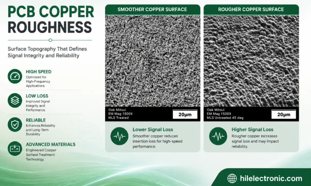
PCB Copper Roughness: Signal Loss, Material Selection and Manufacturing Control
Table of contentsWhat Is PCB Copper Roughness?How Copper...
800G Optical Module PCB Manufacturing and Assembly Service
Table of contentsWhat Makes an 800G Optical Module PCB...
112G PCB Material Selection and High-Speed PCB Manufacturing
Table of contentsWhat “112G PCB Material” Actually...
77 GHz Radar PCB Material Selection and Manufacturing Guide
Table of contentsWhat 77 GHz Changes in a PCBCommon 77 GHz...
How to get a quote for PCBs
Let us run DFM/DFA analysis for you and get back to you with a report.
You can upload your files securely through our website.
We require the following information in order to give you a quote:
-
- Gerber, ODB++, or .pcb, spec.
- BOM list if you require assembly
- Quantity
- Turn time
In addition to PCB manufacturing, we offer a comprehensive range of electronic services, including PCB design, PCBA (Printed Circuit Board Assembly), and turnkey solutions. Whether you need help with prototyping, design verification, component sourcing, or mass production, we provide end-to-end support to ensure your project’s success. For PCBA services, please provide your BOM (Bill of Materials) and any specific assembly instructions. We also offer DFM/DFA analysis to optimize your designs for manufacturability and assembly, ensuring a smooth production process.