
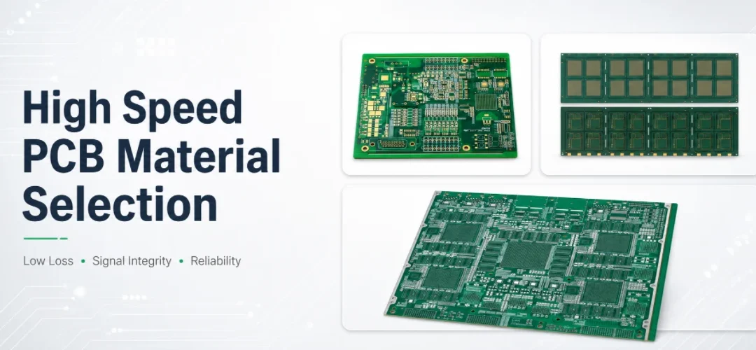
Electronic Circuit Board Production by Highleap in China

Selecting the right PCB production partner can significantly impact quality, cost, and the scalability of your product. This guide will provide insights into the complex process of PCB production, highlight areas where design adjustments can reduce costs, and explain how quality assurance ensures reliability in every board produced.
1. Core Steps in Electronic Circuit Board Production
The PCB production process is both complex and precise, requiring multiple coordinated steps to achieve the final product:
- Design and DFM Review: Initial designs undergo a Design for Manufacturability (DFM) review, where engineers verify that the design can be manufactured efficiently without risking quality. A thorough DFM review helps prevent issues in later stages that could lead to costly redesigns or production delays.
- Material Selection: The choice of materials (e.g., FR4, aluminum, or Rogers laminates) directly impacts the board’s performance and cost. Each material offers specific electrical, thermal, and mechanical properties, which need to be matched with the board’s intended application.
- Layer Stackup and Lamination: For multilayer boards, manufacturers arrange multiple layers and adhere them together through a controlled lamination process. Precision in stackup configuration is crucial for signal integrity and overall performance.
- Drilling and Via Formation: Drilling forms the necessary holes and vias for electrical connectivity between layers. This step includes various types of vias, such as through-hole, blind, and buried, which increase in cost as they become more complex.
- Etching and Plating: Etching removes excess copper from the board to create the traces, while plating adds conductive layers to via holes, ensuring electrical connectivity between layers.
- Soldermask Application and Silkscreen Printing: The soldermask, typically green, protects the copper traces from oxidation and helps prevent short circuits. Silkscreen printing adds markings, component labels, and other details for assembly.
- Surface Finishing: Surface finishes (e.g., HASL, ENIG) protect exposed copper pads, improving solderability and extending board lifespan. The choice of finish affects cost and should align with specific environmental and performance requirements.
- Testing and Quality Assurance: Every board undergoes rigorous quality checks, including Automated Optical Inspection (AOI), in-circuit testing, and sometimes X-ray inspection for complex multilayer boards.
The complexity of these steps increases based on design specifications, materials, and special requirements, which directly affect the production cost and lead time.
2. Key Considerations for Cost-Effective PCB Production
Achieving cost-effective PCB production requires a deep understanding of several critical factors. By carefully managing materials, layer count, finishes, and design choices, engineers can minimize costs without compromising the performance, reliability, or manufacturability of the PCB.
Material Selection: Performance vs. Cost
Material choice significantly impacts both the electrical performance and cost of a PCB. High-performance materials such as Rogers (for high-frequency applications), polyimide (for flexible PCBs), or Teflon (for low-loss, high-speed designs) offer superior electrical, thermal, and mechanical properties but come at a higher cost. These are crucial for demanding sectors like 5G communication, aerospace, and automotive applications.
For more standard applications, FR-4 remains the industry standard due to its affordability and adequate performance for most consumer electronics. However, designers can optimize material costs by using high-performance substrates selectively—such as Rogers in critical signal layers or areas exposed to high temperatures—while leveraging FR-4 or CEM-1 for less demanding layers. Additionally, thermal conductivity and dielectric constant are essential considerations; high-speed or high-power circuits may require materials with specific Dk and Df (dissipation factor) values to ensure signal integrity and heat management.
Layer Count and Stackup Optimization: Reducing Complexity
The number of layers in a PCB directly influences both manufacturing complexity and cost. Adding layers increases the need for precise lamination processes, drilling of vias, and handling of more materials. Therefore, reducing the layer count without compromising functionality is a key cost-saving strategy.
Efficient stackup design plays a pivotal role in minimizing layer count. By consolidating signal and power/ground planes, or by employing buried vias or blind vias selectively, engineers can reduce the overall number of layers while maintaining high-density designs. For high-speed designs, controlled impedance and signal integrity must be carefully managed by optimizing trace widths, spacing, and via placements to ensure reliable performance across fewer layers.
HDI (High-Density Interconnect) designs, while costly, can be beneficial for ultra-compact PCBs, allowing for smaller traces and reduced layer count. However, engineers should weigh the benefits of HDI against the increased cost of microvias and fine-pitch processing.
Surface Finishing: Selecting the Right Option
Surface finish selection directly affects both performance and cost. While finishes like ENIG (Electroless Nickel Immersion Gold) are ideal for high-end applications due to their corrosion resistance and excellent solderability, they involve more complex and expensive processing steps.
For many applications, more economical finishes like HASL (Hot Air Solder Leveling) or OSP (Organic Solderability Preservative) are sufficient. HASL is particularly favored in high-volume production for its ease of application and cost-effectiveness, though it can result in uneven coating on fine-pitch or microBGA (Ball Grid Array) components. For more environmentally-conscious applications, lead-free HASL or immersion silver may be used to comply with RoHS directives.
For PCBs exposed to harsh environments (e.g., high humidity, high temperatures), more durable finishes such as ENIG or immersion gold may be justified despite their higher cost, especially in industries like aerospace, medical devices, and automotive electronics.
Minimizing Over-Engineering: Focused Design for Manufacturability (DFM)
Over-engineering is a common issue when designers focus too heavily on theoretical performance without considering real-world production constraints. A core principle in cost-effective PCB production is Design for Manufacturability (DFM), where designers ensure that every aspect of the PCB design aligns with the manufacturing process to reduce complexities and costs.
Trace width and spacing should adhere to standard guidelines to avoid costly reworks and ensure ease of etching. Via types also play a crucial role; limiting the use of blind and buried vias (which require more intricate drilling) and favoring through-hole vias or via-in-pad designs can reduce costs while maintaining functionality.
Panelization is another essential DFM consideration. By optimizing panel layout for maximum material usage and reducing scrap, manufacturers can significantly lower per-unit costs. Avoiding overhangs and ensuring components fit within the panel’s constraints helps reduce the need for additional routing, cutting, and reworking.

China Highleap Electronic Circuit Board Production
3. Design for Manufacturability (DFM): Streamlining Production and Reducing Costs
Design for Manufacturability (DFM) is a crucial practice in PCB design that ensures designs are optimized for efficient and cost-effective production. By aligning designs with the capabilities of manufacturing processes, DFM helps prevent costly errors, reduce production time, and improve yield rates. Incorporating DFM principles early in the design phase can substantially reduce the risk of design changes and production delays.
Trace Width, Spacing, and Routing Efficiency
One of the foundational DFM principles is optimizing trace width and spacing. Ensuring that traces have standard widths and adequate spacing (according to IPC-2221 or other relevant design standards) simplifies the etching process and reduces the risk of manufacturing defects like signal integrity issues or short circuits. This not only lowers production costs by minimizing errors but also improves the yield rate, which is especially important in high-volume manufacturing.
For high-density designs, where miniaturization or performance considerations drive the need for tighter tolerances, there’s a need to balance complexity with manufacturability. Extremely fine traces or microvias increase the risk of fabrication errors and require advanced inspection techniques, such as automated optical inspection (AOI), leading to higher costs. Minimizing the complexity of the layout by utilizing a more conservative trace width and spacing, where possible, ensures that the design can be efficiently fabricated at scale without costly rework.
Hole Sizes and Via Types: Standardization to Reduce Costs
Optimizing hole sizes and via types is another critical factor in DFM. Standardizing hole sizes to common industry specifications helps streamline drilling processes and reduces tooling costs. More complex hole sizes, such as those used for microvias or blind vias, require more precision and specialized equipment, which increases the overall cost of production.
Through-hole vias are typically less expensive to manufacture compared to blind and buried vias, which require more advanced drilling techniques and precise alignment. Minimizing the number of blind vias and buried vias can significantly reduce both the drilling cost and the complexity of the PCB. Where advanced HDI (High-Density Interconnect) designs are necessary, designers should prioritize via-in-pad or microvia technologies only where their benefits (e.g., for high-speed signals or miniaturized designs) justify the added expense.
Panelization: Maximizing Material Use and Reducing Production Costs
Panelization is another essential aspect of DFM that directly impacts material utilization and cost. Efficient panelization ensures that multiple PCBs can be processed together in a single manufacturing run, minimizing waste and maximizing material yield. By designing panels that optimize the arrangement of PCBs, designers can reduce scrap rates and make better use of the available material.
Designers should consider edge clearance, component layout, and routing paths when designing the panel. Ensuring components do not overhang the edges of the PCB prevents the need for custom spacers or complex routing operations, which can add unnecessary costs. If components or traces extend beyond the edges of the panel, additional steps such as cutting and routing become necessary, which increase both the labor and material costs.
Furthermore, nesting optimization (the process of fitting multiple designs into a panel) can minimize unused areas and reduce the per-unit cost of manufacturing. Proper panelization also improves the efficiency of processes such as soldering and testing, as multiple boards can be handled in parallel.
DFM Best Practices for High-Volume Runs
Implementing DFM best practices becomes even more critical when scaling from prototyping to high-volume production. Design decisions made during the prototyping phase can have a significant impact on manufacturing costs and lead time during mass production. By adhering to DFM guidelines, designers can avoid costly redesigns and last-minute changes, ensuring smoother transitions to full-scale production.
Additionally, DFM helps to enhance yield rates, ensuring that the number of usable boards per production batch is maximized. By designing for manufacturability, engineers can identify potential production issues early in the design phase, which minimizes the risk of defects and reduces scrap rates during assembly, inspection, and testing.

4. Quality Assurance: Ensuring Reliability and Longevity
In critical industries such as automotive, aerospace, and medical devices, the reliability and longevity of PCBs are non-negotiable. The need for stringent quality assurance (QA) processes is paramount to ensure that each PCB meets the highest performance standards while maintaining durability across its lifecycle. Implementing effective QA protocols reduces the risk of failure and guarantees that the PCBs will perform as expected, even under extreme conditions.
Testing Procedures: Identifying Defects Early
A robust testing regimen is essential in ensuring that the PCB functions correctly and meets all operational requirements. Several testing methods are employed to identify defects at different stages of production:
-
Automated Optical Inspection (AOI): AOI uses high-resolution cameras and software to inspect the PCB’s surface for defects such as solder bridge issues, misalignment, or damaged traces. This process is essential for detecting defects early in the manufacturing process, ensuring that only high-quality boards move forward.
-
Flying Probe Testing: This method uses moving probes to contact PCB pads and test electrical continuity, identifying open circuits, short circuits, and component failures. Flying probe testing is particularly useful for small batch runs or prototypes, where creating a dedicated test fixture might be too costly.
-
In-Circuit Testing (ICT): ICT verifies the functionality of each individual component on the PCB by checking for resistance, voltage, and current within the circuits. It ensures that components are properly placed, soldered, and functioning as expected.
-
X-Ray Inspection: For multilayer PCBs or boards with complex BGA (Ball Grid Array) or CSP (Chip Scale Package) components, X-ray inspection is often used to inspect hidden connections and solder joints that are not visible through traditional testing methods. This method is critical for detecting voids in solder joints or misalignments that could lead to failure over time.
Certifications and Industry Standards
In regulated industries, certifications and adherence to recognized standards are critical to maintaining product integrity and regulatory compliance. Some of the most important certifications include:
-
ISO 9001: This global quality management standard ensures that the PCB manufacturer has robust processes in place for consistent product quality and continual improvement. An ISO 9001 certification demonstrates the manufacturer’s commitment to meeting customer expectations and quality requirements.
-
IPC Standards: The IPC (Institute for Printed Circuits) provides a set of standards—such as IPC-2221 for PCB design and IPC-A-600 for PCB inspection—that define the quality criteria for different aspects of PCB production, including design, materials, and testing. Adhering to IPC standards ensures that PCBs meet the highest industry benchmarks for reliability and performance.
-
RoHS Compliance: For products sold in the European Union and many other regions, RoHS (Restriction of Hazardous Substances) compliance is required. This certification ensures that PCBs are free from certain harmful substances, such as lead, mercury, and cadmium, and aligns with global environmental standards.
-
UL Certification: Underwriters Laboratories (UL) certification for PCBs is required for certain industries, particularly in applications where fire resistance or electrical safety is critical. UL certifications such as UL 94 (flammability rating) and UL 746E (material properties) ensure that the PCB materials and assembly processes meet strict safety criteria.
Environmental Durability: Materials and Finishes for Harsh Conditions
Many PCBs are exposed to challenging environmental conditions, including extreme temperatures, moisture, vibrations, and corrosive elements. For these applications, environmental durability is a key consideration in the manufacturing process.
-
Temperature Resistance: In applications such as automotive and aerospace, where temperature fluctuations are extreme, high-temperature laminates (e.g., polyimide, BT resin) are used to ensure the board can withstand thermal cycling without warping or degrading. These materials help the PCB maintain its electrical properties and structural integrity over time.
-
Moisture Resistance: In environments where humidity is a concern (e.g., marine or outdoor applications), conformal coatings such as silicone, acrylic, or polyurethane are often applied to protect the PCB from moisture-induced damage. Additionally, waterproof enclosures and specialized surface finishes like immersion gold or ENIG can provide enhanced protection against corrosion.
-
Vibration and Shock Resistance: For applications in military or automotive sectors, rigid-flex PCBs or highly robust FR-4 materials are used to prevent cracking or failure due to vibration or shock. These materials are often paired with reinforced layers or potting techniques to further protect the board.
-
Corrosion Resistance: In harsh industrial environments (e.g., oil and gas), silver or gold-plated finishes are often used for their superior resistance to corrosion and wear. These finishes ensure that the PCB maintains a reliable electrical connection despite exposure to chemicals, humidity, or saltwater.
By choosing the appropriate materials and finishes, manufacturers can ensure that the PCBs are well-suited to their intended operating environment, reducing the likelihood of premature failures and costly repairs.
5. Scaling from Prototyping to Volume Production
PCB production needs vary widely depending on the stage of development. From rapid prototyping to full-scale production, each phase has distinct requirements:
- Prototyping and Small Batches: For initial development, rapid prototyping allows designers to validate designs quickly and make adjustments. Flexibility in production volumes, quick turnaround times, and close collaboration with the manufacturing team are essential during this stage.
- Volume Production and Cost-Saving Opportunities: As products move to mass production, economies of scale help reduce costs. Working with a PCB manufacturer who offers scalable solutions and consistent quality across production volumes ensures smooth transitions and cost savings.
- Supply Chain Management: Establishing a reliable supply chain and inventory management process is critical for volume production. Manufacturers who can source materials, maintain inventory, and offer flexible lead times contribute to supply chain stability and reduce production risks.
This flexibility between prototyping and volume production helps support product timelines, from development to market launch.
6. Choosing the Right PCB Manufacturing Partner
Selecting a PCB manufacturing partner that aligns with your specific requirements is crucial for efficient and reliable production. At Highleap Electronics, we embody the key attributes you should look for:
-
Engineering Support and DFM Expertise: Our team offers one-on-one engineering support, guiding designers through DFM practices to identify changes that enhance manufacturability and reduce costs.
-
Advanced Production Capabilities: We specialize in complex designs, including HDI, rigid-flex production, and fine-pitch processing. Our extensive experience with these technologies ensures seamless compatibility with your design specifications.
-
Commitment to Quality: Highleap Electronics is dedicated to quality, backed by industry certifications, rigorous testing, and continuous process improvement, which ensures consistent output and minimizes field failures.
By partnering with Highleap Electronics, you gain access to tailored solutions and expert guidance that meet industry standards, regulatory compliance, and cost control, empowering your projects to succeed.
Conclusion
Effective electronic circuit board production requires attention to detail at every stage, from design and material selection to panelization and testing. By following best practices in DFM, choosing appropriate materials, and collaborating with a manufacturing partner who prioritizes quality and customer support, engineers and product developers can achieve cost-effective and high-performance PCBs.
For those seeking tailored solutions, our team at Highleap Electronics offers one-on-one consultations with experienced engineers. We can help you navigate complex design and production requirements, ensuring your project stays on budget and meets performance standards. Reach out to us to explore how our production expertise and commitment to quality can bring your designs to life with efficiency and precision.
Get a Free PCB & PCBA Quote

Recommended Posts
ITEQ IT-968G PCB for High-Speed Switch and Radar Designs
ITEQ IT-968G sits in the practical middle of the...
ITEQ IT-988GSE PCB for Ultra-Low-Loss 100G and 400G Backplanes
An IT-988GSE PCB should be selected from the channel loss...
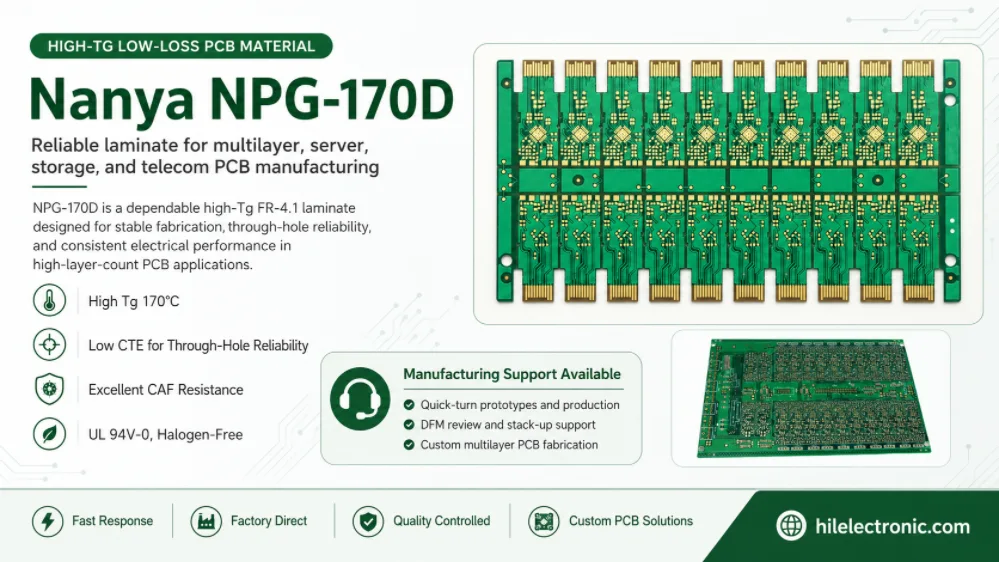
Nanya NPG-170D PCB Manufacturing for High-Tg Multilayers
Nanya NPG-170D PCB manufacturing should be planned as a...

Panasonic MEGTRON 7N PCB Manufacturing for High-Speed HDI
Panasonic MEGTRON 7N PCB manufacturing is a high-speed...
How to get a quote for PCBs
Let us run DFM/DFA analysis for you and get back to you with a report.
You can upload your files securely through our website.
We require the following information in order to give you a quote:
-
- Gerber, ODB++, or .pcb, spec.
- BOM list if you require assembly
- Quantity
- Turn time
In addition to PCB manufacturing, we offer a comprehensive range of electronic services, including PCB design, PCBA (Printed Circuit Board Assembly), and turnkey solutions. Whether you need help with prototyping, design verification, component sourcing, or mass production, we provide end-to-end support to ensure your project’s success. For PCBA services, please provide your BOM (Bill of Materials) and any specific assembly instructions. We also offer DFM/DFA analysis to optimize your designs for manufacturability and assembly, ensuring a smooth production process.