
One-Stop Service for Electronic Device PCB Manufacturing and Assembly

In today’s fast-paced world of technology, electronic device PCBs are at the core of every device we use. Whether it’s a smartphone, a medical instrument, a consumer appliance, or an industrial control system, PCBs serve as the foundational component connecting and supporting all other electronic parts. At Highleap Electronic, we specialize in the manufacturing and assembly of these vital components, helping businesses create reliable, efficient, and high-performance electronic devices.
What is an Electronic Device PCB?
A PCB is an essential part of nearly all electronic devices. It acts as the platform that physically supports and electrically connects the components of the device, such as resistors, capacitors, microchips, and transistors. In its simplest form, a PCB is a flat board made of an insulating material, usually fiberglass, with conductive copper traces that form the electrical pathways connecting components.
In more complex devices, PCBs come in various designs and forms, such as single-layer, multi-layer, and flexible PCBs. Regardless of the configuration, the primary role of the PCB remains the same: to provide a reliable, compact, and efficient way for components to interact within the electronic system. Highleap Electronic offers complete solutions for electronic device PCB manufacturing and assembly. From design to installation, we ensure high-quality, reliable, and efficient PCBs for your devices.
The Key Role of PCBs in Electronic Devices
PCBs are often considered the “heart” of an electronic device due to their critical role in ensuring the device operates efficiently. Here’s a closer look at why PCBs are so important:
-
-
Mechanical Support: The PCB physically holds all the electronic components together, ensuring that they are securely mounted and connected. This is especially critical in modern electronic devices, where miniaturization has resulted in smaller, more compact designs.
-
Electrical Connectivity: The copper traces on the PCB create pathways that allow electricity to flow between components. This ensures that signals, power, and data are transmitted precisely as needed. Without a PCB, there would be no reliable way to interconnect the components in an organized manner.
-
Signal Integrity: The design of a PCB significantly impacts the integrity of the signals passing through the device. Proper PCB design ensures that signals travel with minimal distortion and interference, which is particularly important in high-speed applications like smartphones, computers, and telecommunications devices.
-
Heat Management: Modern electronic devices generate a significant amount of heat. High-quality PCBs are designed with materials and structures that help dissipate this heat, preventing components from overheating and ensuring the longevity of the device.
-
Durability and Reliability: The robustness of a PCB is crucial for the overall durability of an electronic device. PCBs must be able to withstand environmental factors like temperature fluctuations, humidity, and physical stresses, ensuring that the device functions reliably over time.
-
Electronic Device PCB Manufacturing Process: From Concept to Final Product
1. Concept and Idea
The creation of a high-quality electronic device PCB begins with the initial concept and idea phase. During this stage, engineers and designers collaborate to understand the functional requirements of the final product. Key considerations include the purpose of the device, the type of components required, and the overall design specifications. By thoroughly understanding the project requirements, a solid plan is laid out to move forward into the design and production stages, ensuring that the final PCB aligns with both performance and cost goals.
2. PCB Design
Once the concept is established, the next phase is PCB design. This involves using specialized design software (such as Altium Designer or Eagle) to map out the layout of the PCB. During this step, the placement of electronic components (resistors, capacitors, microchips, etc.) is determined, and the copper traces that will connect the components are routed. The design must also take into account factors such as signal integrity, heat dissipation, and power distribution. The design is carefully reviewed and optimized to ensure the PCB will meet the required functional, mechanical, and electrical specifications.
3. PCB Manufacturing
After the PCB design is finalized, the next step is PCB manufacturing. This stage involves producing the physical board based on the design layout. The process starts by selecting the appropriate materials, such as FR4 (fiberglass) for the substrate and copper for the conductive traces. The layers of copper and insulating material are laminated and etched to form the desired circuit patterns. If the PCB is multi-layered, additional layers are stacked and connected via vias (small holes) to establish electrical connections between layers. The manufacturing process also involves drilling holes for component leads and vias, which are crucial for the proper assembly of components.
4. PCB Testing
Once the PCB is manufactured, it undergoes testing to ensure it functions correctly. The testing phase is critical in identifying any defects or issues that may have occurred during manufacturing. Electrical tests, such as in-circuit testing (ICT), are conducted to verify that the copper traces are correctly connected and that there are no short circuits or open circuits. Functional testing is also performed to ensure that the PCB performs as expected under normal operating conditions. Any issues discovered during testing are addressed before proceeding to the next stage.
5. PCB Assembly
The next step is PCB assembly, where the components are mounted onto the PCB. This is typically done using automated machines, such as pick-and-place robots, which precisely position the components onto the board. After the components are placed, they are soldered onto the PCB using reflow soldering, a process that melts solder paste and creates strong, reliable electrical connections. Other soldering techniques like wave soldering may also be used for specific components. Once the assembly is complete, a visual inspection or automated optical inspection (AOI) is conducted to ensure that all components are properly soldered and positioned.
6. PCB Validation
After assembly, the PCB undergoes validation. This stage ensures that the assembled board meets the design specifications and works as intended. The validation process often involves rigorous functional testing under real-world conditions. Any issues that may arise during this process are addressed through debugging and troubleshooting. If the PCB passes all the validation tests, it is then prepared for the final steps, ensuring the design’s electrical and mechanical performance meets the required standards.
7. PCB Packaging
Once validated, the next step is PCB packaging. This phase ensures that the PCB is securely packed to avoid any damage during shipping or handling. Anti-static bags and shock-absorbing materials are often used to protect the sensitive components from electrostatic discharge (ESD) and physical damage. Proper packaging ensures that the PCB arrives at its destination in perfect condition, ready for installation into the final product. Clear labeling and documentation are also included for easy identification during the installation process.
8. PCB Installation in the Device
The final step in the electronic device PCB manufacturing process is installation in the device. After packaging and shipping, the PCB is installed into its respective electronic device. This could be a consumer product, industrial equipment, medical device, or any other application that requires the PCB. The installation process involves connecting the PCB to other internal components, such as power supplies, displays, and connectors. Once installed, the entire device undergoes a final system-level test to ensure that the PCB functions correctly in the context of the complete system, ensuring the device performs reliably.
The process of designing, manufacturing, testing, assembling, and installing a high-quality electronic device PCB involves numerous steps that require expertise and precision. At Highleap Electronic, we follow a rigorous and structured approach to ensure that every PCB we produce meets the highest standards of performance, durability, and reliability. Whether you’re working on consumer electronics, industrial machinery, or medical devices, our PCB solutions are designed to power the next generation of electronic devices.

Key Applications of Electronic Device PCBs
PCBs are used in a wide range of electronic devices across various industries. Here are some examples of how electronic device PCBs power modern technology:
1. Consumer Electronics
Smartphones, tablets, laptops, and televisions all rely on highly sophisticated PCBs to function. These devices require PCBs that support high-speed data transfer, power management, and signal integrity, all while being compact and durable.
2. Medical Devices
In medical technology, PCBs are used in devices like ECG machines, ultrasound scanners, and pacemakers. These devices require ultra-reliable PCBs that ensure accurate measurements, signal processing, and patient safety.
3. Automotive Electronics
Modern vehicles are packed with electronic systems, including engine control units (ECUs), infotainment systems, and advanced driver-assistance systems (ADAS). High-performance PCBs are used to interconnect these components and ensure the vehicle operates smoothly and efficiently.
4. Industrial Automation
In industrial settings, PCBs are used in equipment like programmable logic controllers (PLCs), motor drives, and sensors. These devices rely on PCBs to manage complex processes and ensure the seamless operation of machinery and systems.
5. Internet of Things (IoT) Devices
IoT devices, such as smart thermostats, security cameras, and wearable technology, are powered by compact PCBs that allow for connectivity, data transmission, and power management in small, energy-efficient packages.
Conclusion
The electronic device PCB is an integral component that enables the functionality and performance of modern technology. As a leader in PCB manufacturing and assembly, Highleap Electronic is committed to delivering high-quality, reliable, and innovative PCBs for a wide range of industries. Whether you are developing consumer electronics, automotive systems, or medical devices, our expertise ensures that your devices will meet the highest standards of quality and performance.
Get a Free PCB & PCBA Quote

Recommended Posts
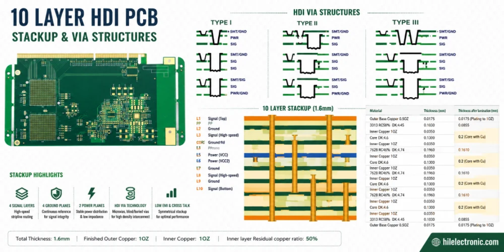
10 Layer HDI PCB Engineering for Microvias and BGA Escape
Figure 1. 10 layer HDI PCB engineering for microvias and...

8 Steps to Manufacture a Perfect Aluminum PCB
Figure 1. Aluminum Pcb manufacturing reference for PCB...

Outdoor Lighting PCB Manufacturing & Assembly by Highleap Electronics
Figure 1. outdoor lighting PCB production and assembly...

Lighting PCB Manufacturer: PCB Fabrication, PCB Assembly & Turnkey LED Lighting
Figure 1. Lighting PCB manufacturer overview for LED light...
How to get a quote for PCBs
Let us run DFM/DFA analysis for you and get back to you with a report.
You can upload your files securely through our website.
We require the following information in order to give you a quote:
-
- Gerber, ODB++, or .pcb, spec.
- BOM list if you require assembly
- Quantity
- Turn time
In addition to PCB manufacturing, we offer a comprehensive range of electronic services, including PCB design, PCBA (Printed Circuit Board Assembly), and turnkey solutions. Whether you need help with prototyping, design verification, component sourcing, or mass production, we provide end-to-end support to ensure your project’s success. For PCBA services, please provide your BOM (Bill of Materials) and any specific assembly instructions. We also offer DFM/DFA analysis to optimize your designs for manufacturability and assembly, ensuring a smooth production process.