
Power Supply Filter PCB Design for EMI Control

One-stop power supply filter PCB: layout review, material selection, EMI simulation, scalable production, faster compliance & lower failure rates. EMI failures usually surface when prototypes are expensive and schedule buffers are gone. Hidden pitfalls—fragmented ground pours, oversized X capacitors shifting resonance, misaligned common‑mode choke placement—cascade into failed scans and redesign cycles. This article gives you a repeatable path: map dominant noise sources, set frequency‑band insertion loss targets, build stable impedance networks, minimize loop areas, and validate early using near‑field probing plus pre‑scan. Follow the framework and turn certification uncertainty into a controlled checklist.
Common Mode Choke vs Differential Mode Filter Selection
Most engineers understand the theory, but practical power supply filter PCB implementation is where designs succeed or fail. Common-mode noise travels on both conductors in the same direction, returning through ground. Differential-mode noise appears between conductors. Each requires different filtering approaches.
Common-mode filtering essentials:
- Current-compensated chokes provide high impedance without saturation
- Y-capacitors shunt common-mode current to chassis ground
- Placement near noise source or victim improves effectiveness
- Keep Y-cap ground connections short—long traces add inductance
Differential-mode filtering realities:
- Standard inductors work but watch saturation current
- X-capacitors between line conductors filter differential noise
- Two-stage filters outperform single-stage with same component count
- Damping prevents resonance with source/load impedance
For a recent AC-DC Converter PCB project, separating common-mode and differential-mode filtering improved attenuation by 20dB while using fewer components. These principles apply equally to Switch Mode Power Supply PCB filter design.
Where to Place EMI Filter Components on PCB
Filter component placement impacts performance more than component values. A perfectly calculated filter performs poorly with suboptimal layout. Place filters where current naturally flows, not where convenient for PCB routing.
Input filter placement hierarchy:
- Common-mode choke immediately after input connector
- X-capacitors between phases after the choke
- Y-capacitors from each phase to chassis ground
- Differential inductors if additional filtering needed
- Second stage repeats pattern for high-attenuation requirements
Never place filter components where they couple noise around the filter. We’ve seen designs where poor placement allowed noise to bypass expensive filters entirely. For power supply filter PCB layouts, maintain at least 10mm separation between input and output sides of filters. Similar spacing rules apply to Power Inverter PCB filter sections.
How to Connect Filter Ground in Power Supply PCB
Ground loops destroy filter performance and create new noise problems. The solution isn’t eliminating grounds—it’s controlling where current flows. Strategic ground plane splits and connections force current through intended paths.
Effective grounding techniques:
- Single-point chassis ground connection prevents loops
- Separate filter ground planes from circuit grounds
- Connect grounds at filter output, not randomly
- Use ground planes for shielding, not current carrying
For Power Electronics PCB designs with multiple filter stages, cascade ground connections from clean to dirty sections. This prevents contamination of filtered power.
Power Supply Filter Design for MHz Switching Frequencies
As switching frequencies increase, traditional filters become less effective. Parasitic inductance in capacitors and capacitance in inductors limit high-frequency performance. Modern designs require specialized components and techniques.
High-frequency solutions:
- Use feedthrough capacitors for frequencies above 100MHz
- Implement ferrite beads for GHz-range filtering
- Select capacitors with self-resonant frequency above target range
- Multiple parallel capacitors with different values broaden effective range
Three-terminal capacitors outperform standard two-terminal types above 10MHz. For applications switching at MHz frequencies, conventional filters need supplementing with high-frequency components. These techniques are crucial for High Efficiency Power PCB designs using GaN or SiC devices.

Active EMI Filter Circuit for Variable Speed Drives
Passive filters work well for fixed-frequency noise, but switching power supplies generate variable-frequency harmonics. Active filters adapt to changing noise profiles, providing superior performance in dynamic conditions.
Active filter implementation tips:
- Sense noise before passive filter for feedforward control
- Use high-speed op-amps with adequate gain-bandwidth
- Implement stability compensation to prevent oscillation
- Combine with passive filters for broadband attenuation
We helped design an active power supply filter for variable-speed motor drives that reduced harmonics by 40dB across the entire operating range—impossible with passive filters alone. These advanced techniques also benefit DC-DC Converter PCB applications with varying switching frequencies.
How to Test Power Supply EMI Filter Performance
Measuring filter performance requires proper test setups. Standard network analyzers don’t account for source and load impedances affecting real-world performance. LISN (Line Impedance Stabilization Networks) provide standardized impedances for conducted emissions testing.
Practical testing approaches:
- Measure with actual source and load, not just 50Ω systems
- Test across temperature range—component values drift
- Verify performance with maximum rated current flowing
- Check for resonances causing gain instead of attenuation
Our PCB assembly services include filter characterization using calibrated test equipment. Pre-compliance testing during development prevents certification failures.
Reducing EMI Filter Cost in Power Supply Design
Filter components, especially safety-rated capacitors and custom magnetics, significantly impact product cost. Strategic design choices reduce costs while maintaining performance.
Cost reduction strategies:
- Use standard components in non-critical positions
- Implement PCB-based inductors for low-current applications
- Share common-mode chokes between multiple channels
- Optimize filter order—sometimes less is more
For volume production, custom integrated filters reduce assembly cost and improve consistency. Our PCB fabrication and electronic manufacturing service teams help optimize filter designs for manufacturing efficiency.
Trust Highleap Electronics for power supply filter PCB solutions that ensure EMI compliance without breaking budgets. We understand the balance between performance, cost, and manufacturability.
FAQs — Power Supply Filter PCB
What PCB materials are recommended for power supply filter PCBs?
For most filter PCBs, standard high-Tg FR-4 is appropriate and cost-effective. For designs operating at unusually high switching frequencies where parasitic loss matters, consider low-loss FR-4 variants (e.g., Isola or Panasonic families). Pure RF laminates (Rogers, etc.) are generally unnecessary for typical SMPS filter work.
This guide covers EMI filtering and noise control on power input or converter boards. For the broader power supply PCB overview, use power supply circuit board overview; for trace geometry, return paths, and controlled signals, compare the design with controlled impedance review.
How should I choose X and Y capacitors for safety and performance?
Select X-rated (X1/X2) capacitors for line-to-line use and Y-rated (Y1/Y2) for line-to-earth; ensure they meet the required safety class for your application (e.g., X2 for mains across many consumer uses, Y1 for direct connection to earth in high-safety contexts). Prioritize low-ESR, appropriate voltage rating, and place them so their lead/traces are short to minimize parasitics.
How do I size a common-mode choke for a power supply filter PCB?
Size chokes by rated continuous current, required differential and common-mode impedance at target frequency, and saturation margin for inrush/surge events. Also check DC resistance (DCR) tradeoffs—lower DCR reduces I²R loss but may require larger cores.
How should filters handle inrush and surge currents?
Design filters to tolerate worst-case inrush: choose chokes with high saturation current, use thermally robust capacitors, and consider NTCs or soft-start circuits upstream of the filter. Ensure surge margins so filter components don’t saturate or fail during startup or fault conditions.
What PCB manufacturing considerations improve filter reliability?
Specify adequate annular rings and pad sizes for high-current parts, use teardrops on power traces, define solder mask clearance for Y caps and safety parts, and request controlled impedance where needed. Also plan test points for filter validation and include assembly instructions for polarized/safety components.
Which simulation tools help predict filter performance?
Use circuit simulators (LTspice, PSpice) for time-domain behavior and filter tuning; use S-parameter/network analysis tools (Keysight ADS, Qucs, or EM solvers) to predict high-frequency parasitics and coupling. Co-simulation of source/load impedance yields the most realistic results.

Related Articles
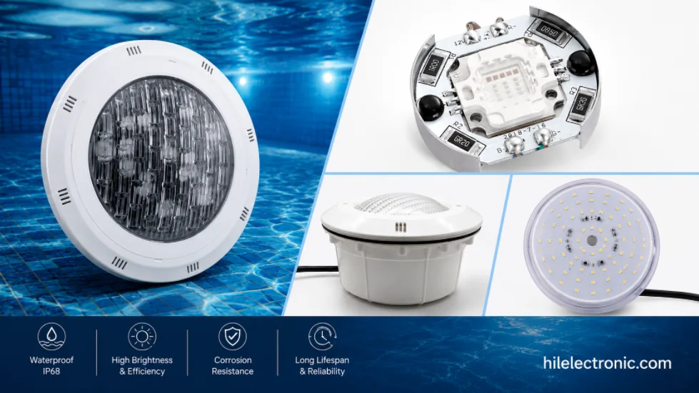
Underwater & Pool LED Light PCBs: IP68 Potted Boards, Low-Voltage Drivers & Safety
Figure 1. LED pool light PCB manufacturing reference....
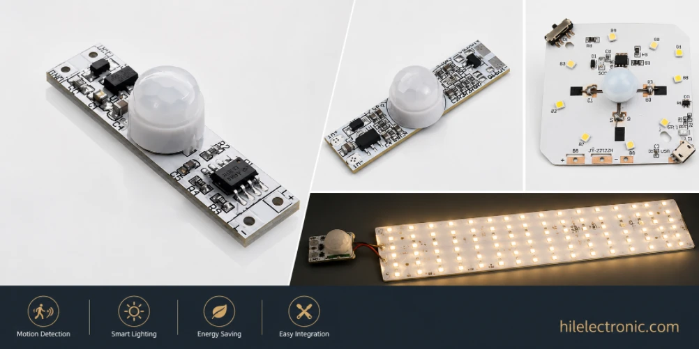
Motion Sensor & Smart LED Light PCBs: Sensor, Control, Driver & Wireless Boards
Figure 1. motion sensor LED light PCB manufacturing...
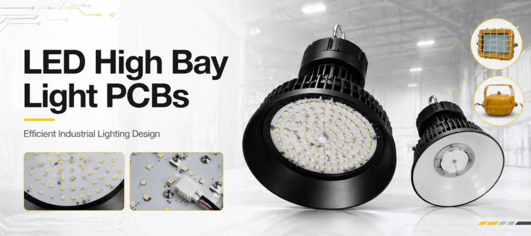
LED High Bay Light PCBs: Metal-Core Light Engines, Drivers & Turnkey Boards Built to Spec
Figure 1. LED high bay light PCB manufacturing reference....
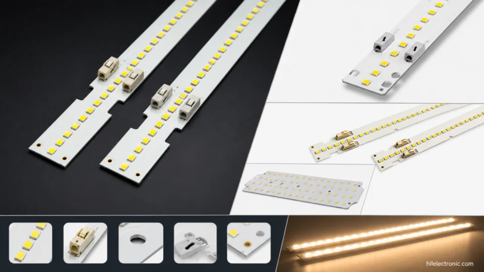
LED Linear & Strip Light PCBs: Long-Format Engines, Flexible & Rigid-Flex Boards
Figure 1. LED linear light PCB manufacturing reference....
How to get a quote for PCBs
Let us run DFM/DFA analysis for you and get back to you with a report.
You can upload your files securely through our website.
We require the following information in order to give you a quote:
-
- Gerber, ODB++, or .pcb, spec.
- BOM list if you require assembly
- Quantity
- Turn time
In addition to PCB manufacturing, we offer a comprehensive range of electronic services, including PCB design, PCBA (Printed Circuit Board Assembly), and turnkey solutions. Whether you need help with prototyping, design verification, component sourcing, or mass production, we provide end-to-end support to ensure your project’s success. For PCBA services, please provide your BOM (Bill of Materials) and any specific assembly instructions. We also offer DFM/DFA analysis to optimize your designs for manufacturability and assembly, ensuring a smooth production process.