
DBC Substrate Prototype Builds and PCB Assembly Support

DBC substrate prototypes are commonly used to verify thermal behavior, insulation performance, and assembly compatibility before full production. These early builds help identify design or process risks and reduce issues during later manufacturing stages. Highleap Electronics provides PCB fabrication and assembly support for DBC-based projects, with DFM review and coordinated sourcing when required.
Table of Contents
A DBC substrate prototype is typically used when a design needs quick validation before committing to production tooling and long term supply. For EV and HEV traction inverters, OBC and DC DC converters, fast chargers, industrial motor drives, energy storage, and renewable energy conversion, prototype builds make it practical to verify thermal behavior, insulation margins, mechanical interfaces, and assembly compatibility while design changes are still easy to implement.
Highleap Electronics is a PCB manufacturing and PCB assembly factory. We are not positioned as a direct DBC substrate manufacturer. Our value is helping teams move from prototype validation to production delivery by combining DFM review, PCB fabrication services, and turnkey assembly, while coordinating DBC substrate sourcing when a qualified supplier is required for your specification. Programs that include ceramic circuit requirements often pair DBC with other build types, and teams frequently evaluate ceramic PCB fabrication options alongside their substrate plan.
1. DBC substrate prototype overview
A DBC substrate prototype is a small quantity build of DBC substrates intended for design validation, functional testing, and early reliability evaluation. Unlike a cost optimized volume run, prototyping prioritizes speed and flexibility so you can iterate without waiting for high MOQs and long production windows. Teams usually prototype to answer a few fundamental questions early.
- Thermal verification confirms that heat spreading and junction to case behavior match simulation and cooling assumptions
- Electrical robustness checks isolation performance and clearance margins under real voltage stress
- Assembly readiness validates that surface finish and metallization choices match the intended attachment and interconnect process
- Mechanical fit verifies interfaces to housings, heat sinks, and clamping structures while tolerances are still adjustable
Prototype planning is easier when stakeholders align on the bonding approach and process limits early, which is why many teams map their design choices to the underlying DBC process before releasing a first article build.
2. DBC substrate prototype specifications
Clear specifications reduce iteration cycles and protect schedule. A practical DBC substrate prototype specification should cover material selection, copper definition, surface finish intent, and mechanical limits that affect handling and assembly. The goal is not to over specify every detail but to lock the few items that determine whether a prototype can be assembled and tested without surprises.
2.1 Ceramic material selection
Ceramic choice sets the baseline for thermal conductivity, mechanical toughness, and cost. Many teams start with alumina for early learning cycles, then move to higher performance ceramics when power density and reliability targets tighten.
- Alumina Al2O3 is widely available and cost effective for many industrial designs and early evaluation builds
- Aluminum nitride AlN supports higher thermal conductivity when heat flux is the limiting factor
- Silicon nitride Si3N4 offers high mechanical strength and is often considered for aggressive cycling environments
Material decisions are easier when the team agrees on the expected thermal load and cycling profile, and many projects capture those assumptions alongside the substrate definition.
2.2 Copper thickness and copper layout intent
Copper thickness and pattern geometry influence current handling, thermal spreading, and mechanical stress concentration. Prototyping is the stage where teams confirm that copper choices support both electrical performance and manufacturability.
- Common copper thickness options include 0.127mm 5 mil, 0.254mm 10 mil, 0.3mm, 0.508mm 20 mil, and 0.635mm 25 mil
- Single sided or double sided copper bonding is selected based on insulation design and heat flow strategy
- Pattern details should avoid sharp stress risers and unsupported long thin copper features when thermal cycling is critical
2.3 Surface finish aligned to attachment and interconnect
Surface finish is one of the most common causes of prototype rework because it directly impacts solderability, wetting behavior, and bonding stability. Defining finish intent up front prevents mismatches between the substrate and the assembly process.
- ENIG is commonly selected for stable solderability and corrosion resistance during prototype handling
- Nickel gold variants are frequently used when wire bonding is part of the interconnect plan
- Silver plating is often specified when sintered silver die attach is part of the process route
2.4 Dimensions flatness and edge quality
Mechanical limits determine how a substrate behaves during printing, placement, bonding, and clamping. Even when the electrical design is correct, flatness and edge quality can drive assembly yield and handling damage. A good prototype specification defines the minimum needed constraints so the build can move through fixtures reliably.
- Unit size and panel format should match fixture concepts and assembly flow
- Flatness targets should align with printing and placement capability
- Edge quality requirements help prevent chipping during shipping and handling

3.DBC substrate prototype workflow
A fast prototype cycle depends on clean inputs and quick engineering feedback. Most projects move through three practical steps that reduce iteration time while keeping the build aligned to scale up requirements.
3.1 File package and build intent
- Gerber files, DXF outline, and mechanical drawings for unit definition
- Material and finish choices based on the intended assembly route
- Prototype quantity and target ship window
- Short application context that clarifies voltage, thermal load, and assembly plan
3.2 DFM review and risk reduction
DFM feedback focuses on what will prevent a prototype from assembling cleanly. It usually covers minimum feature limits, copper geometry that may concentrate stress, finish compatibility with attachment, and mechanical elements that can conflict with fixtures or clamping.
3.3 Build delivery and learning loop
After delivery, teams typically run assembly trials and targeted tests, then feed results into the next revision. Prototyping works best when each iteration answers a clear question so the design converges quickly.
4. PCB fabrication and PCB assembly for DBC based systems
DBC substrates rarely ship as standalone parts. Many power electronics products include control boards, driver boards, sensing circuits, and communication interfaces that must be manufactured and assembled with stable quality. Highleap Electronics supports these needs with scalable PCB fabrication and turnkey PCBA so the substrate work connects to a complete manufacturable system.
- PCB fabrication supports rigid PCBs, HDI, heavy copper, and other stackups used in power electronics and control circuitry
- PCB assembly supports SMT and through hole processes, mixed technology builds, and production workflows that scale from prototype lots to volume
- System consistency improves when PCB build, assembly planning, and inspection criteria are aligned early through DFM review
Programs that require ceramic circuit options beyond DBC often consider AMB and DPC as part of the technology decision. Highleap Electronics supports these needs as a China-based ceramic PCB manufacturing partner, and our China ceramic PCB manufacturing capabilities help teams compare process routes and move from evaluation builds into stable production.

5. Volume manufacturing and volume assembly
Once the DBC substrate prototype is validated, the priority shifts from fast learning to stable delivery. Volume readiness comes from locking key specifications, confirming repeatable assembly results, and building a supply plan that supports production schedules. Highleap supports this transition with volume PCB fabrication and volume PCBA, and we also support mass production for other PCB types used across industrial and consumer electronics.
- Pilot builds confirm process stability and early yield before full scale release
- Volume PCB fabrication delivers consistent production for rigid, flex, rigid flex, HDI, and heavy copper designs
- Volume PCB assembly supports repeatable SMT and through hole processes with inspection and testing aligned to your acceptance criteria
- Supply simplification reduces schedule risk when PCB fabrication and assembly are coordinated under one factory workflow
Teams comparing substrate suppliers often keep selection criteria documented, and the topic aligns naturally with how a qualified DBC substrate manufacturer is evaluated for consistency and reliability.
6. DBC substrate prototype RFQ checklist
A complete RFQ package helps reduce back and forth and protects lead time. If your build includes PCB fabrication and assembly, sending everything together usually shortens the total schedule because DFM feedback can address the full system instead of one part at a time.
- Design files Gerber, DXF outline, and PDF drawings
- DBC definition ceramic type, thickness, copper thickness, surface finish
- Quantity prototype quantity and expected production volume
- Timeline target ship date and milestone needs
- Assembly intent soldering, die attach, wire bonding, handling constraints
- Testing requirements continuity, insulation, and functional testing if required
Many teams keep DBC terminology and material context in their internal documentation, and the same content is often anchored by a practical overview of direct bonded copper substrate definitions and the broader DBC substrate scope used during early project planning.

Recommended Posts

Wireless Mechanical Keyboard PCB Manufacturing
Table of contentsWireless Keyboard PCB Procurement...

Split Keyboard PCB Manufacturing & Assembly
Table of contentsSplit Keyboard PCBA Procurement...
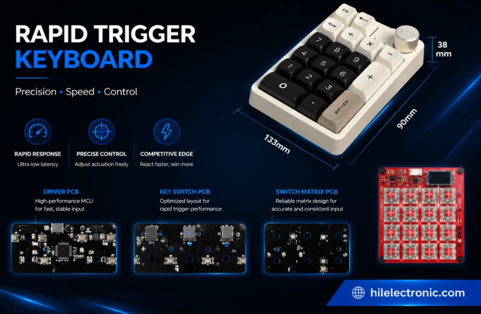
Rapid Trigger Keyboard PCB Manufacturing & PCBA
Table of contentsRapid Trigger PCBA Buying and Performance...
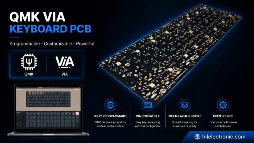
QMK/VIA Keyboard PCB Manufacturing & Assembly
Table of contentsQMK/VIA Keyboard PCB Buying...
How to get a quote for PCBs
Let us run DFM/DFA analysis for you and get back to you with a report.
You can upload your files securely through our website.
We require the following information in order to give you a quote:
-
- Gerber, ODB++, or .pcb, spec.
- BOM list if you require assembly
- Quantity
- Turn time
In addition to PCB manufacturing, we offer a comprehensive range of electronic services, including PCB design, PCBA (Printed Circuit Board Assembly), and turnkey solutions. Whether you need help with prototyping, design verification, component sourcing, or mass production, we provide end-to-end support to ensure your project’s success. For PCBA services, please provide your BOM (Bill of Materials) and any specific assembly instructions. We also offer DFM/DFA analysis to optimize your designs for manufacturability and assembly, ensuring a smooth production process.