
High-Speed PCB for Robotics: PCIe, DDR, MIPI and Ethernet Layout
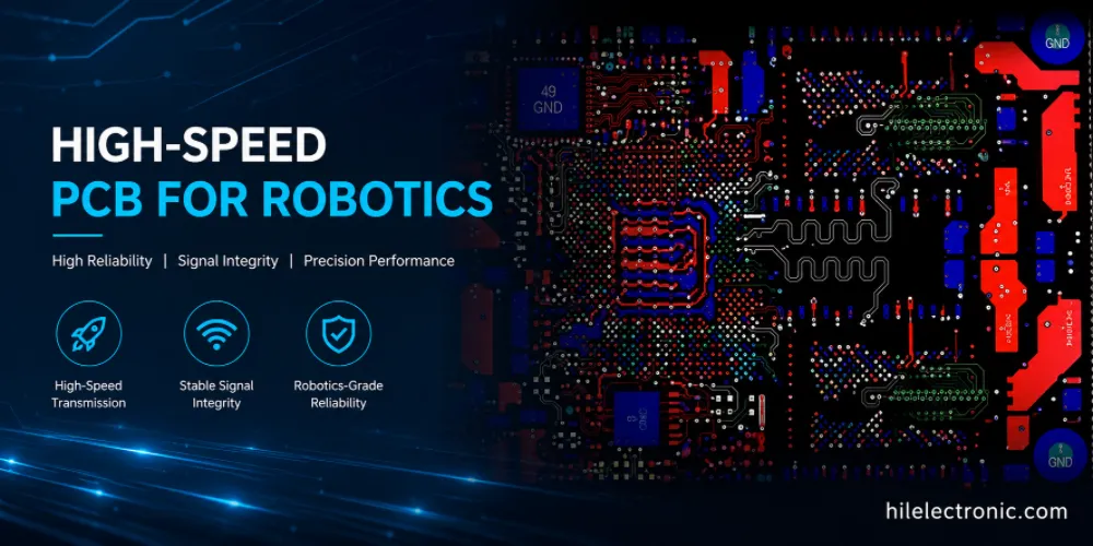
High-speed PCB manufacturing for robotics supports data paths such as PCIe, DDR, MIPI CSI-2, USB 3.x, Ethernet, LVDS, HDMI, and high-speed camera links. These interfaces are common in robot vision, AI compute, communication, control boards, and sensor fusion systems.
This guide is written from a PCB fabrication and PCBA perspective. A high-speed robot PCB is not defined only by fast chips; it depends on controlled impedance, stackup accuracy, material selection, via transitions, return paths, assembly quality, test planning, and production repeatability.
When Robotics Products Need High-Speed PCB Manufacturing
Data Bandwidth in Modern Robots
Modern robots rely on cameras, AI processors, sensors, drives, and communication links that move large amounts of data. A robot vision board may use MIPI CSI-2; a compute board may use PCIe and DDR; a communication board may use gigabit Ethernet; a sensor fusion system may combine several interfaces on one PCB.
High-speed PCB manufacturing becomes necessary when signal edge rates, not only clock frequencies, make routing and fabrication important. Even moderate data rates can fail if return paths, impedance, or via transitions are poorly controlled.
Why Manufacturing Precision Matters for High-Speed Performance
High-speed design depends on the actual manufactured stackup. Dielectric thickness, copper thickness, trace width, solder mask, copper roughness, and material tolerance affect impedance and loss. If the board is fabricated differently from the design model, simulation assumptions may no longer hold.
The topic overlaps with robot vision and camera PCB design, robot communication PCB design, HDI PCB for robotics, and robot PCB fabrication control. Robotics teams should align electrical design with fabrication capability before routing is finalized.
PCIe, DDR, MIPI CSI-2, Ethernet, USB, and Camera Interface Risks
Differential Pair and Parallel Bus Requirements
PCIe, USB, Ethernet, MIPI, and LVDS use differential routing with impedance and length-control requirements. DDR memory also requires timing control across address, command, clock, and data groups. Each interface has different tolerance, topology, and reference-plane needs.
Routing rules should define impedance targets, length matching, via limits, spacing from aggressors, reference planes, and connector transitions. The manufacturing notes should identify controlled-impedance nets clearly so the fabricator can build and measure them correctly.
Camera and AI Compute Board Challenges
Robot camera and AI boards often combine high-speed interfaces with compact packaging and thermal density. MIPI camera routing, PCIe accelerator links, memory buses, and processor power rails may all compete for layer count. BGA PCB assembly and HDI fanout are common in these designs.
When high-speed routing is combined with compact mechanical requirements, the board may need HDI, low-loss materials, or both. The decision should be based on channel length, data rate, connector choice, and product volume.
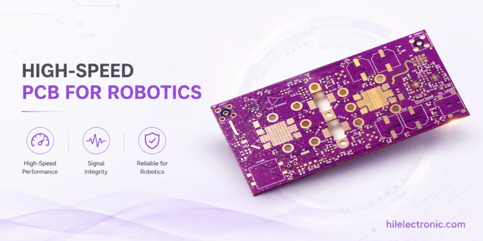
Stackup, Controlled Impedance, Materials, and HDI Decisions
Controlled Impedance and Return Path Discipline
Controlled impedance is a fabrication requirement, not just a layout setting. The PCB stackup must define dielectric thickness, copper weight, trace width, spacing, and impedance tolerance. Continuous reference planes are essential; plane splits and poor via transitions can create reflections and noise.
For production, impedance coupons or measurement methods may be specified. The need depends on interface speed, product risk, and customer requirements. High-speed robot PCBs should not rely on undocumented stackups.
Material Selection and HDI Trade-Offs
Standard FR-4 may be adequate for short, moderate-speed channels. Higher data rates, longer channels, or low-loss requirements may need mid-loss or low-loss laminates. Material choice should be matched to actual channel loss rather than selected by assumption.
HDI can improve fanout and reduce routing stubs, but it adds cost. HDI PCB cost control should be considered early when choosing between more layers, HDI buildup, smaller packages, and low-loss material.
PCBA Assembly, BGA, Inspection, and Functional Testing
Fine-Pitch Assembly and X-Ray Inspection
High-speed robotics boards often use BGA processors, memory, FPGAs, connectors, and small passives. Assembly quality affects signal behavior when solder joints, voiding, or connector alignment are marginal. BGA packages may require X-ray inspection and controlled reflow profiles.
Assembly drawings should identify critical packages, keep-out areas, thermal pads, shield cans, and any press-fit or board-to-board connectors. Without clear documentation, production may pass visual inspection while still creating high-speed failures.
Functional Test for High-Speed Interfaces
Not every production fixture can run full compliance tests, but it should verify boot, memory detection, communication links, camera interface presence, Ethernet function, USB function, firmware identity, and current consumption. Test coverage should catch assembly defects that affect high-speed operation.
For complex boards, bring-up logs and serial-number records are useful. They help distinguish layout issues, component issues, firmware issues, and assembly variation during pilot production.
Signal Integrity, Power Integrity, EMC, and Thermal Reliability
SI and PI Must Be Reviewed Together
Signal integrity depends on impedance, loss, crosstalk, stubs, reference planes, and termination. Power integrity depends on regulator placement, decoupling, plane impedance, current return paths, and switching noise. In robotics compute boards, SI and PI failures can look like random software instability.
High-speed boards should reserve layout room for decoupling, test access, and thermal paths. Optimizing only for compactness can reduce margin and make the board difficult to debug.
EMC and Thermal Risk in Dense High-Speed Boards
High-speed edges and switching regulators can create emissions. Poor return paths can also make the board more susceptible to noise from motors and power systems. robot PCB EMI and EMC design should be considered before the robot reaches certification testing.
Thermal density is another risk. Processors, memory, PHYs, and AI modules can heat small areas of the PCB. robot PCB thermal management planning should include copper spreading, thermal vias, heatsink contact, and enclosure conduction.
Prototype, Validation, and Production Transfer for High-Speed Boards
Prototype With Production-Intent Stackup
High-speed prototypes should use the intended stackup and material where possible. A cheaper prototype stackup may not validate impedance, insertion loss, crosstalk, or via behavior. If a substitute stackup is used, the difference should be documented clearly.
Debug access should be planned before layout completion. Test pads, headers, and measurement access are harder to add after dense routing is finished.
Pilot Production and Yield Measurement
Pilot builds should measure impedance results, assembly yield, BGA inspection findings, boot failures, interface failures, and thermal observations. This data shows whether the high-speed board is manufacturable, not just functional.
Before production release, the team should freeze stackup, material, BOM alternates, firmware, test method, and any impedance requirements. Uncontrolled changes can invalidate previous validation.
RFQ Package Details That Improve Quotation Accuracy
For a high-speed robotics PCB RFQ, include interface list, stackup target, impedance requirements, length-matching constraints, BGA package details, material preference, test requirements, and any simulation or coupon expectations.
- PCIe, DDR, MIPI, USB, Ethernet, LVDS, or camera net classes
- single-ended and differential impedance targets
- material class and loss budget where known
- BGA fanout, via strategy, and HDI requirements
- power rail sequencing and current expectations
- functional test coverage for boot, memory, and high-speed links
Production Release Checks Before Scaling
Before release, the high-speed board should use a production-intent stackup. Changing dielectric thickness, copper weight, material family, or via structure after validation can change signal integrity.
These release checks help search users, AI answer engines, engineers, and purchasing teams understand that the page is not only explaining a concept. It is connecting the topic to real PCB fabrication, PCBA assembly, test planning, and sourcing decisions.
Common Design and Manufacturing Mistakes to Avoid
Common high-speed robot PCB mistakes include routing to generic rules, using a non-final stackup for prototype validation, crossing reference-plane splits, ignoring power integrity, and adding test pads after dense routing is complete.
- controlled-impedance nets not identified in the fabrication notes
- stackup and material changed after signal validation
- BGA fanout reviewed without assembly yield input
- DDR, PCIe, MIPI, or Ethernet constraints not separated by net class
- no plan for boot, memory, and interface functional testing
- thermal solution added after high-speed layout is complete
Highleap Electronics High-Speed Robotics PCB Manufacturing and Assembly Support
What the Manufacturing Package Should Include
Highleap Electronics reviews PCB fabrication data, assembly files, BOM details, and test requirements before production. For high-speed robotics pcb, the RFQ package should include Gerber or ODB++ files, stackup target, impedance requirements, interface list, BGA details, BOM, pick-and-place, assembly drawing, test requirements, firmware instructions, and expected production volume. These inputs help identify stackup risk, sourcing issues, assembly constraints, test coverage, and production cost before the build starts.
A complete package also reduces email back-and-forth. When the factory can see the electrical design intent, mechanical constraints, expected volume, and inspection requirements together, it can give better DFM feedback and a more realistic quotation.
How Highleap Helps Convert Design Intent Into Buildable PCBA
High-speed robotics boards are sensitive because fabrication tolerance, assembly quality, BGA fanout, power integrity, EMC, and thermal density all influence real product behavior. Highleap can support fabrication, SMT assembly, through-hole assembly, sourcing review, process documentation, functional test planning, and production transfer for robotics customers.
For PCIe, DDR, MIPI, Ethernet, USB, camera, or AI compute boards, the manufacturing package can be reviewed for high-speed PCB and PCBA risks. Request a PCB manufacturing and assembly review.
What Buyers Should Check Before Choosing a PCB/PCBA Supplier
High-speed PCB buyers should evaluate stackup review, impedance control, HDI capability, BGA assembly, and functional test planning together. A supplier that only quotes layer count may miss the manufacturing details that affect high-speed behavior.
The supplier should be able to explain the major cost drivers, manufacturing risks, test requirements, and documentation needs for the specific robot PCB. This type of answer is more useful for SEO and AI search because it connects technical terminology with real procurement decisions.
High-Speed PCB for Robotics FAQs
What is a high-speed PCB in robotics?
It is a robot PCB carrying fast interfaces such as PCIe, DDR, MIPI CSI-2, USB 3.x, Ethernet, LVDS, HDMI, or high-speed camera data.
When does a robotics PCB need controlled impedance?
Controlled impedance is needed when signal speed, edge rate, or interface requirements make trace geometry and reference planes critical to reliable communication.
Is FR-4 enough for high-speed robot PCBs?
Sometimes. Short moderate-speed channels may use FR-4, while longer or faster channels may require mid-loss or low-loss materials.
Why do high-speed PCBs often use HDI?
HDI helps fan out fine-pitch BGAs, reduces routing stubs, saves area, and can improve signal paths for compact robotics compute and vision boards.
How are high-speed robot PCBs tested?
Testing may include impedance verification, boot test, memory detection, interface checks, Ethernet or USB function, camera link checks, current measurement, and thermal observation.
What causes high-speed PCB failures in robots?
Common causes include poor impedance control, plane discontinuities, via stubs, crosstalk, weak power integrity, BGA assembly defects, connector loss, and EMC noise.

Recommended Posts

Isola Astra MT77 PCB Manufacturing
Figure 1. Isola Astra MT77 PCB ManufacturingIsola Astra...

Nelco N4000-13 PCB Material and Manufacturing Guide | Highleap Electronics
Figure 1. Nelco N4000-13 PCBNelco N4000-13 PCB is a...

Copper Clad Laminate: Complete Material Selection Guide for PCB Engineers
Every electrical property that matters in a printed...

Inside a China Ceramic PCB Factory: Process Control Across Power/LED/RF/Medical
Table of Contents Inside a China Ceramic PCB Factory: How...
How to get a quote for PCBs
Let’s run DFM/DFA analysis for you and get back to you with a report. You can upload your files securely through our website. We require the following information in order to give you a quote:
-
- Gerber, ODB++, or .pcb, spec.
- BOM list if you require assembly
- Quantity
- Turn time
For PCBA services, please provide your BOM (Bill of Materials) and any specific assembly instructions. We also offer DFM/DFA analysis to optimize your designs for manufacturability and assembly, ensuring a smooth production process.