
LCP PCB Manufacturer for High-Frequency and Compact Electronic Products
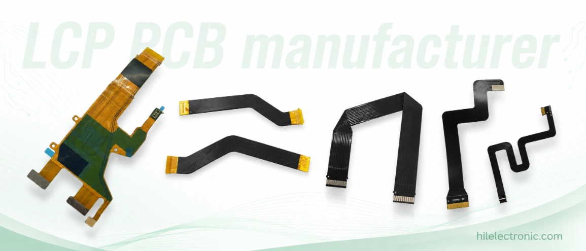
The phrase “LCP PCB manufacturer” covers several very different products: a thin antenna film, a fine-line interconnect, a multilayer thermoplastic module or a hybrid circuit. A useful supplier assessment must therefore be construction-specific. Equipment ownership alone does not show that a factory can control the selected LCP film, copper interface, dimensional movement, via formation and assembly support.
Highleap reviews LCP projects as qualification programs. The first response should identify the proposed material route, the features that set electrical or mechanical performance, and the first-article evidence required before volume transfer. Capabilities are confirmed after file and material review rather than expressed as universal minimum line, via or layer-count claims.
How to Qualify an LCP PCB Manufacturer
A capable supplier should be able to explain the production route before accepting the order. The explanation does not need to disclose proprietary process settings, but it should identify how the material will be stored, supported, imaged, drilled, metallized, laminated and inspected. Vague claims such as “we process all flexible materials” are not enough because LCP behaves differently from conventional thermoset constructions.
| Qualification question | Why it matters | Evidence to request |
|---|---|---|
| Has the factory reviewed the exact LCP grade and copper construction? | Different films, claddings and bonding systems do not share one process window. | Written stackup review and material-availability confirmation. |
| How will panel movement be compensated? | Thin LCP constructions can change dimension during thermal and mechanical processing. | First-article dimensional report or scaling plan. |
| How are vias formed and metallized? | Laser parameters, surface condition and adhesion affect microvia reliability. | Via structure proposal, microsection criteria and test method. |
| Can the factory inspect fine lines and RF-critical geometry? | Small dimensional changes can alter impedance or antenna response. | AOI/measurement plan and critical-feature list. |
| Can fabrication and assembly be planned together? | Thin panels often need carriers, fixtures and controlled support during SMT. | Panel drawing, fixture concept and assembly DFM feedback. |
Highleap does not publish a universal minimum line, microvia size or layer count for every LCP job because those limits depend on film thickness, copper, panel format, via type and acceptance standard. The responsible answer is construction-specific. Customers can send preliminary files for review before completing the purchase specification.
Can a conventional flex PCB factory process LCP?
Some flex-circuit equipment is useful, but equipment ownership alone does not prove process capability. LCP surface preparation, adhesion, dimensional control and lamination can require different settings and validation. A factory that regularly processes polyimide may still need a trial lot for an unfamiliar LCP system. This is not a weakness; it is a sign that the supplier distinguishes material qualification from general marketing.
Which documents should a professional buyer request?
At minimum, request confirmation of the exact material, stackup, copper, via method, surface finish, inspection scope and permitted substitutions. For high-reliability or RF projects, add microsection, impedance, insertion-loss or functional coupon requirements as appropriate. If the project will move to volume production, define lot traceability and change-control rules before the first article is approved.
The Manufacturing Steps That Are Different on LCP
LCP is valued in part for its electrical and moisture behaviour, but those same material characteristics do not eliminate fabrication risk. Thin films need stable support. Surface condition affects adhesion. Thermal exposure can move the panel. Fine features need controlled etching. Laser vias require process development. Multilayer bonding needs a construction-specific cycle. The factory must manage the sequence as one system.
Material handling and surface preparation
Material identity and storage history should be checked when the lot is received. Clean handling is important because contamination can reduce adhesion or create cosmetic defects in transparent or thin areas. Surface treatment must promote metallization or bonding without damaging the film. Highleap confirms the supplier’s processing guidance and the customer’s cleanliness requirements before releasing an unfamiliar construction.
Fine-line imaging and dimensional compensation
LCP is often chosen for compact products, so the artwork may contain fine pitch, narrow gaps and tight antenna geometry. The panel must remain supported during imaging and etching. Artwork scaling should be based on the actual material and process sequence. The design should identify which dimensions are electrically critical so compensation does not accidentally change a resonator, feed line or coupling gap.
Where the project combines high wiring density with small vias, review the broader high-density interconnect PCB requirements as well as the material. LCP does not remove the need for capture-pad tolerance, via-to-copper spacing, plating continuity and sequential-lamination planning.
Laser via formation and metallization
Laser energy, focus, debris removal and landing-pad condition must match the film and copper. A visually open via can still have poor metallurgical quality if residue remains or the interface is damaged. Microsection criteria should define plating continuity, void limits and interface condition. For unusual via size or aspect ratio, Highleap may recommend a process coupon before the product panel is released.
The project can also use the site’s laser-drilled PCB guidance to distinguish a manufacturable microvia from an aspirational drill table.
Multilayer bonding
Multilayer LCP may use thermoplastic fusion or another approved bonding approach depending on the product system. Temperature, pressure, surface condition, copper topography and panel support influence the final bond line and registration. It is unsafe to copy a polyimide rigid-flex press cycle into an LCP drawing without material-vendor and fabricator review. The release should identify exact materials and the required finished dielectric spacing rather than prescribing an unverified generic cycle.
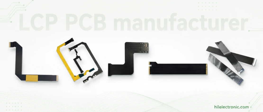
Matching the LCP Process to the Final Product
The word “application” is useful only when it changes the manufacturing plan. An antenna circuit may prioritise dielectric consistency, line geometry, copper profile and RF testing. A wearable sensor may prioritise thinness, moisture resistance, bend behaviour and biocompatible packaging requirements outside the PCB itself. A high-density module may prioritise microvias, fine pitch and assembly coplanarity. A medical or aerospace product may add traceability, cleanliness and documentation.
LCP antenna and high-frequency circuits
For an LCP antenna PCB, the quotation should identify operating frequency, critical antenna and feed dimensions, ground-clearance rules, solder-mask keep-outs, surface finish and any RF acceptance method. A generic impedance note cannot replace an antenna performance plan. Highleap can fabricate the geometry and provide agreed coupons or dimensional reports, while final radiated performance normally belongs to the assembled module and enclosure.
Readers comparing substrate families can review high-frequency PCB materials, but the comparison must remain construction-specific. LCP may offer advantages for thin, integrated or moisture-sensitive products; it is not automatically the lowest-cost or simplest route for every RF board.
Miniaturized sensors and compact modules
Fine conductors, small pads and thin panels create assembly challenges. Fiducials, tooling, component clearances and carrier design should be agreed before panelisation. If the module includes a shield frame, connector or overmoulding step, the mechanical drawing should show loads and keep-outs. Dimensional stability should be evaluated over the actual thermal sequence, including assembly and any downstream process.
Wearable and flexing products
LCP can be used in flexible structures, but bend life depends on the full conductor and layer construction. The project still needs bend lines, radius, cycle expectation and support features. Do not infer dynamic-flex performance from the polymer name. Where movement is critical, create a representative mechanical coupon and validate it under the intended environment.
Start an LCP PCB Project With Highleap
The fastest route to a defensible quotation is a staged review. First, send the material data, stackup and artwork. Second, identify the critical electrical and mechanical features. Third, agree on prototype quantity and inspection. Fourth, release volume production only after the first article demonstrates that the construction and process are stable.
- Exact LCP material designation, supplier data and permitted alternatives.
- Layer stackup, copper construction, final thickness and panel or unit format.
- Gerber/ODB++, drill, mechanical drawing and controlled dimension list.
- Impedance, RF, via, adhesion, bend or dimensional test requirements.
- Prototype quantity, annual demand and target schedule.
- BOM, centroid, assembly drawing, programming and functional-test data for PCBA.
Highleap can combine LCP board fabrication with component sourcing and assembly when the design is suitable for the available process. Thin circuits may require carrier fixtures and a specific panel format; these are included in DFM rather than discovered after bare-board completion. Assembly input should follow the PCB assembly file requirements so the quotation covers tooling, inspection and testing accurately.
Material stock determines whether a project can use quick-turn production. Once construction and stock are confirmed, prototype and low-volume schedules can be planned. Payment terms and international shipping are stated in the quotation. After delivery, Highleap can review issues using lot records, approved artwork and inspection data. For an RF project, agreed RF PCB testing or dimensional evidence should be defined before production so both parties judge the result against the same criteria.
Assembly fixtures should be part of the supplier audit
An LCP circuit can be thin enough to move during solder-paste printing, placement and reflow. A supplier offering turnkey PCBA should explain how the panel is supported and how the fixture avoids covering components, fiducials or heat-sensitive areas. The carrier design should also permit inspection and depanelisation without damaging the circuit.
Highleap reviews panel size, tooling, fiducials, component mass and reflow direction before assembly. For modules with shields, connectors or overmoulding, downstream mechanical operations are added to the review. This is particularly important when the LCP circuit is part of a compact three-dimensional assembly rather than a flat board.
Cleanliness and surface condition can be product requirements
High-frequency, sensor and medical-related assemblies may have cleanliness limits beyond normal visual acceptance. The RFQ should identify ionic cleanliness, residue, particle or cosmetic requirements where relevant. Cleaning chemistry and process temperature must be compatible with the material, finish and components. A broad “clean board” note is not a measurable standard.
If the product uses wire bonding, conductive adhesive or sensitive sensing surfaces, the pad finish and contamination limits should be defined before quotation. Highleap can then determine whether the required process and verification are available or whether an external specialist step is needed.
Supplier changes require more than a purchasing approval
LCP films and clad constructions can differ in thickness, copper adhesion, dimensional movement and electrical data. A material substitution may require revised compensation, laser parameters, lamination and RF modelling. The customer should therefore freeze the exact product or define a qualification route for alternatives.
For repeat production, Highleap records the approved stackup and material source. If supply changes, the factory can present the proposed construction and affected controls. Depending on product risk, a dimensional coupon, microsection, RF measurement or assembly first article may be needed before the new source is released.
Cost should be separated into material, process and evidence
LCP PCB cost can be driven by material yield, fine-line imaging, laser drilling, sequential lamination, inspection, assembly fixtures and test. Buyers should ask for these items to be visible. A lower unit price may omit microsection, controlled impedance or first-article reporting that another quotation includes.
Prototype pricing is also different from stable volume pricing because the first lot may carry engineering and tooling cost. Once the construction and compensation are approved, scheduled production can use repeat tooling and a defined process route. Highleap can quote both stages so the buyer understands the cost of qualification and the expected recurring price.
Professional after-sales support depends on retained evidence
If an LCP assembly fails in the field, the cause may involve material, via, assembly, enclosure stress or environment. Lot traceability, dimensional records, microsections and functional-test data help narrow the cause. Highleap retains the approved files and production record within the agreed quality system so reported issues can be investigated technically rather than handled as a simple sales dispute.
Fine-pitch component assembly needs pad and finish coordination
LCP modules often use small passives, RF front-end devices, sensors or fine-pitch packages. Pad dimensions, solder mask, finish and stencil apertures should be reviewed together. A finish chosen only for the bare board may create assembly variation, while an assembly-driven pad change can alter RF parasitics. Highleap coordinates DFM across fabrication and PCBA when both services are ordered.
For very thin circuits, board support and thermal mass influence reflow. The process may require a dedicated carrier and controlled cooling. AOI can inspect visible joints; X-ray may be needed for hidden terminations. Functional testing is quoted only when fixtures, software and limits are defined.
Mechanical integration should be supplied with the PCB files
Compact LCP circuits may be folded, bonded, inserted into a housing or laminated into another subassembly. The factory needs the final mechanical state to plan outline, stiffeners, adhesive areas and packaging. If a metal frame or plastic overmould is applied later, pressure and temperature can affect the circuit.
A 3D drawing or section view is often more useful than several pages of generic tolerances. Highleap can review critical interfaces before tooling and flag features that cannot be inspected after assembly.
Acceptance criteria should be product-specific
An antenna circuit may need dimensional and RF evidence. A sensor may need cleanliness and leakage requirements. A fine-line interconnect may prioritise continuity, microvia integrity and coplanarity. Applying every available test increases cost and can still miss the actual risk. The RFQ should select evidence that corresponds to the product function.
How to evaluate an LCP prototype supplier before volume transfer
Ask whether the supplier can reproduce the approved stackup, scaling and via route after several months. Review its change-control process and whether production records identify material and tooling revision. A prototype that relies on undocumented manual adjustment can be difficult to transfer to volume.
Highleap records the approved project data and can prepare repeat quotations using the released construction. If a process or material change is required, the impact is communicated before production. This continuity is important to professional buyers seeking a long-term LCP PCB factory rather than a one-time sample shop.
Capability note: LCP products vary widely. Minimum geometry, layer count, via structure and lead time are confirmed only after the exact material system and design files are reviewed.

Recommended Posts

TMM4 Filter PCB Manufacturing
TMM4 filter PCB manufacturing is controlled by the...

TMM3 PCB Manufacturing for RF Modules
TMM3 PCB manufacturing is most useful where the RF module...

TMM6 PCB Fabrication
TMM6 fabrication is the process-control page for a mid-Dk...

TMM10 PCB Manufacturing for Compact RF Designs
Table of contentsHow TMM10 Shrinks RF StructuresTMM10 vs...
How to get a quote for PCBs
Let’s run DFM/DFA analysis for you and get back to you with a report. You can upload your files securely through our website. We require the following information in order to give you a quote:
-
- Gerber, ODB++, or .pcb, spec.
- BOM list if you require assembly
- Quantity
- Turn time
For PCBA services, please provide your BOM (Bill of Materials) and any specific assembly instructions. We also offer DFM/DFA analysis to optimize your designs for manufacturability and assembly, ensuring a smooth production process.