
Panasonic MEGTRON 7N PCB for AI Server HDI Boards
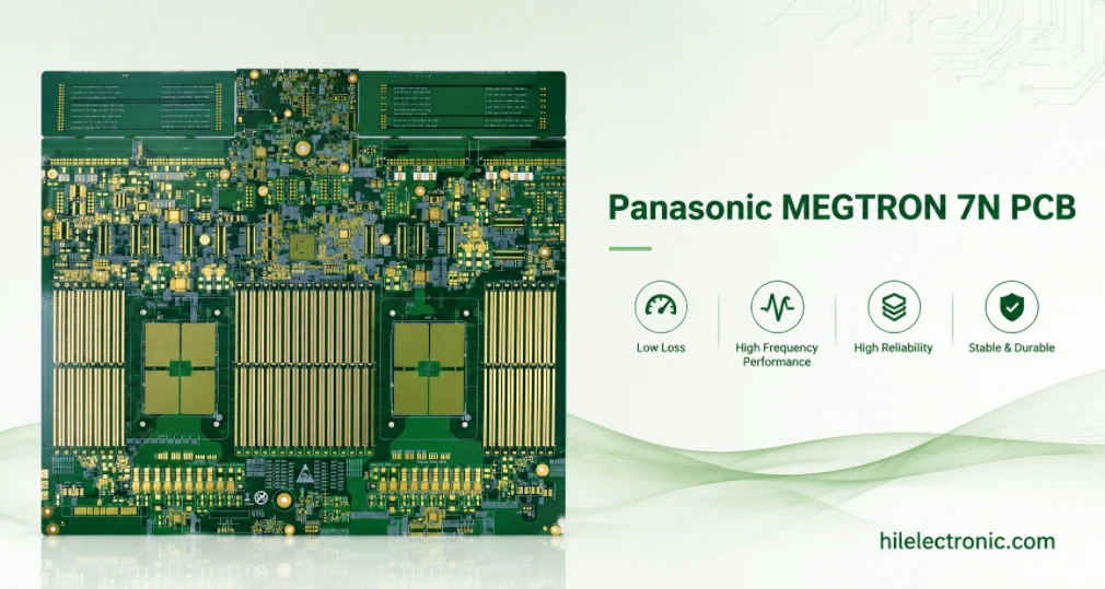
Panasonic MEGTRON 7N is best understood as a platform material for difficult high-speed multilayers, not as a universal “server laminate.” The public Panasonic product is laminate R-5785(N) with prepreg R-5680(N). Panasonic positions the MEGTRON 7 family for high-speed, large-data servers and routers and states that the family is compatible with HDI, very high layer count, and large-format PCB layouts.
The value of MEGTRON 7N becomes clear when electrical and manufacturing demands arrive together: long package-to-package channels, multiple connectors, high layer count, thick finished boards, dense BGA escape, microvias, deep backdrill, large panels, and repeated lead-free assembly. In that environment, the PCB is not a passive carrier. It is a major channel segment whose glass, copper, resin, vias, registration, and process variation must be modeled and controlled.
Panasonic’s public series page lists typical values for R-5785(N)/R-5680(N) including 200°C Tg by DSC, 210°C by DMA, 400°C Td, T288 greater than 120 minutes, 42 ppm/°C z-axis CTE below Tg, 0.06% water absorption, and representative Dk/Df data. Panasonic also publishes construction-specific electrical tables for MEGTRON 7N builds; those should drive the released stackup instead of a single family-level number.
Why AI Servers and Large Interconnect Platforms Stress the PCB
AI servers, high-radix switches, routers, storage platforms, and accelerator trays place more devices, memory, power stages, and high-speed connectors on larger, thicker boards. The channel may pass through a package breakout, several stripline layers, a high-speed connector, a midplane or cable assembly, another connector, and a receiver package. At the same time, the board must route thousands of lower-speed nets, carry high current, manage heat, and survive assembly.
| Platform pressure | Electrical consequence | Manufacturing consequence |
|---|---|---|
| Higher lane rate and PAM4 modulation | Less eye margin, higher sensitivity to loss, reflection, crosstalk, and mode conversion. | More stringent stackup, copper, via, connector, and coupon control. |
| Longer reach across chassis or large board | Distributed dielectric and conductor loss become a larger share of the budget. | Large panels, tighter thickness uniformity, more panel-position variation. |
| High connector density | More launch loss, crosstalk, return-path transitions, and mechanical constraints. | Dense drill patterns, press-fit loads, registration and hole-quality demands. |
| High layer count | More routing options but more via transitions and propagation variation. | Thicker board, long barrels, resin-flow complexity, registration accumulation. |
| HDI/BGA density | Shorter escape and fewer through-via stubs are possible. | Sequential lamination, microvia reliability, capture-pad and registration control. |
| High power and thermal mass | Temperature affects loss and reliability; power noise can couple into channels. | Heavy copper, asymmetric structures, warpage, complex reflow and cooling hardware. |
A material decision that looks only at Df misses this interaction. MEGTRON 7N can support a stable low-loss stack, but it cannot compensate for a poor connector, an unbackdrilled stub, an over-rough inner-layer treatment, or a microvia structure that is not mechanically qualified. Architecture, material, layout, and fabrication must be released together.
Treat the Board as Part of the Package-to-Package Channel
At high lane rates, the board contributes distributed attenuation, impedance variation, skew, and phase delay. Every layer assignment determines trace width and field distribution; every copper surface affects conductor loss; every via and connector changes return loss; every glass style influences effective Dk and differential skew. The system simulation should therefore use the proposed production construction before the layout is considered final.
- Define channel classes. Separate short on-board routes, medium card routes, long connectorized paths, and the platform’s worst reach.
- Assign packages and connectors. Use vendor or measured S-parameters with the intended footprint and launch.
- Build layer-specific transmission-line models. Include R-5785(N)/R-5680(N) construction data, copper profile, finished thickness, roughness, and temperature.
- Model all via structures. Include BGA escape, layer changes, backdrill residual stubs, return vias, antipads, and press-fit fields.
- Run process corners. Sweep dielectric thickness, etch, Dk/Df, copper, residual stub, and connector tolerances.
- Allocate margin. Decide whether the board, connector, package, or equalization is the limiting component before selecting a higher material tier.
The longest route should not dictate every layer blindly
A platform may reserve selected low-loss layers for the longest links while using other layers for short routes, clocks, control, and lower-speed buses. This can improve routing and cost, but the material system and lamination must remain coherent. The stackup should identify which layer pairs are qualified for which channel class, with route-length and via-count limits that layout can enforce.
Use Construction-Specific Data, Not One Marketing Number
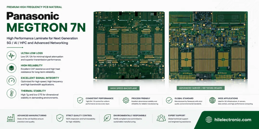
MEGTRON 7N’s construction-specific data are one of its strongest engineering advantages. Dk and Df vary with glass style, resin content, core/prepreg build, and frequency. Panasonic’s family page also shows that similarly named MEGTRON 7 variants and constructions do not share one identical value.
| Data item | Why a family number is insufficient | Release practice |
|---|---|---|
| Dk | Resin-rich and glass-rich constructions have different effective permittivity. | Use the exact core/prepreg table entry or a supplier-confirmed design value for each layer. |
| Df | Frequency, resin/glass ratio, and test method affect loss tangent. | Use frequency-appropriate data and correlate the production line with S-parameter coupons. |
| Pressed thickness | Prepreg resin flow and copper density change the cured dielectric distance. | Release a fabricator stackup based on actual copper percentages and pressed-thickness data. |
| Copper profile | H-VLP, VLP, or other foil options change conductor loss and peel behavior. | Specify the exact foil/profile and include inner-layer treatment in the model. |
| Glass style | Weave changes Dk, skew risk, resin distribution, and manufacturability. | Freeze approved styles and document panel orientation where skew or dimensional behavior matters. |
| Test method | Different methods can produce different apparent Dk/Df. | Do not compare numbers across suppliers unless frequency, specimen, and method are comparable. |
Solve HDI, High Layer Count, and Large Format Together
MEGTRON 7N is often selected precisely because the design needs both high-speed and complex fabrication. HDI stackup design can reduce through-via stubs and improve dense BGA escape, but sequential lamination and stacked microvias add reliability and registration risk. A large-format high-layer board also accumulates dimensional movement across the panel.
| Construction choice | Benefit | Qualification risk |
|---|---|---|
| Blind microvias from outer layer to L2/L3 | Short escape, small discontinuity, routing density. | Laser via diameter, capture, plating, resin fill, corner integrity, thermal cycling. |
| Stacked microvias | Direct vertical escape and compact routing. | Stack alignment, copper fill, interface fatigue; avoid unsupported stacking beyond qualified capability. |
| Staggered microvias | Reduces stacked-interface stress. | Consumes routing area and may add transitions. |
| Deep backdrill on through vias | Removes high-frequency stubs while retaining through-hole fabrication. | Depth control, drill wander, residual stub, pad clearance, panel thickness variation. |
| Sequential lamination | Enables buried vias and dense build-up. | Multiple heat cycles, cumulative registration, resin cure compatibility, warpage. |
| Large panel/high layer count | Improves platform integration. | Center-to-edge registration, dielectric thickness variation, press uniformity, handling damage. |
Choose the simplest via architecture that closes routing
HDI should not be added merely because MEGTRON 7N supports it. A backdrilled through-via solution may be more reliable and economical if it meets the channel. Conversely, a microvia can remove a stub and improve escape where a through via cannot. The via architecture should be chosen from electrical benefit, routing need, and a proven fabrication window.
Registration is an electrical parameter
On a dense BGA or connector field, layer-to-layer registration changes antipad shape, return-path symmetry, and annular ring. On a large board, panel stretch and shrink can vary across position. The first article should map registration and critical via geometry at more than one panel location, and the field-solver model should include realistic offsets for sensitive transitions.
Copper, Microvias, Backdrill, and Connector Density
The material system, copper, vias, and connectors must be co-designed. Low Df reduces dielectric loss, but rough copper can dominate conductor loss on narrow traces; deep backdrill can introduce variation; connector launches can dominate return loss; and press-fit fields can create dense mode-conversion structures.
Copper selection
- Specify the laminate foil profile and the inner-layer adhesion treatment separately.
- Use the lowest-profile foil that meets peel strength, availability, fabrication, and reliability needs.
- Model finished copper thickness and trapezoidal etch geometry, not only base foil.
- Correlate loss with the actual supplier and treatment; the label “VLP” is not a universal roughness model.
- Control foil changes as engineering changes because they alter both loss and impedance.
Backdrill and residual stubs
Backdrill residual-stub targets should include board-thickness variation, drill depth, drill wander, and layer registration. The drawing should define the measurement method and sampling. For the deepest or highest-frequency paths, use a coupon or X-ray/cross-section plan that proves the residual stub without damaging the product.
Connector density
Connector launches should be simulated with the actual MEGTRON 7N stackup, copper, antipad, ground vias, and mechanical keep-outs. A connector vendor reference footprint may need adjustment for the board’s dielectric height and layer count. Press-fit connectors also impose mechanical stress and hole tolerances that must be reconciled with signal-integrity geometry.
MEGTRON 7N Versus MEGTRON 8: Set a Roadmap Boundary
MEGTRON 8 is positioned by Panasonic as a lower-transmission-loss successor for more demanding high-speed channels. That does not make it the automatic choice for every new server. The platform should set a roadmap boundary based on lane rate, reach, connector architecture, and qualification horizon.
| Question | MEGTRON 7N direction | MEGTRON 8 / lower-loss direction |
|---|---|---|
| Does the current worst route pass with guard band? | Remain on MEGTRON 7N and freeze the qualified construction. | Move only if measured or modeled margin is insufficient. |
| Is the next platform 224G PAM4-class or longer reach? | Run a roadmap study; some routes may still pass. | A lower-loss tier may reduce redesign risk and support higher-frequency behavior. |
| Is the board short but highly dense? | MEGTRON 7N may be enough; density may dominate over distributed loss. | Upgrade only if copper/line loss or roadmap justifies it. |
| Are connectors and packages the bottleneck? | Fix or change the interconnect first. | Lower Df may not recover reflection- or connector-dominated margin. |
| Is construction availability and factory experience critical? | Established MEGTRON 7N builds may reduce risk. | New material qualification may add cost, lead time, and yield learning. |
| Does one platform need a long service life and multiple speed generations? | Assess the cost of future redesign or retimers. | A higher tier can be economical when it preserves a long roadmap. |
A fair comparison uses identical layer geometry, copper profile, trace width, connector/via topology, and frequency range. It also includes panel availability, glass styles, UL status, press cycles, qualification data, regional supply, and price. Selecting from one headline Df number can misstate the real channel and production difference.
Do Not Ignore Exact Grade and UL Requirements
The exact suffix and recognition matter. “MEGTRON 7” is a family, and R-5785(N)/R-5680(N) is a specific material pair. Panasonic’s public information also distinguishes N, GN, GE, R, and other grades or constructions. A project that requires a particular UL recognition, flammability status, maximum operating temperature, or customer approval must verify the exact material and stackup rather than assume family-wide equivalence.
- Write laminate and prepreg part numbers on the stackup and purchase documents.
- Confirm the exact UL file/construction and whether the proposed copper, thickness, and build are covered.
- Freeze the IPC slash sheet or customer material class where required.
- Do not substitute another MEGTRON 7 suffix solely because it has similar Dk/Df.
- Confirm regional manufacture, standard panel size, foil, glass, and prepreg availability.
- Retain certificates and lot traceability in the first-article and production records.
Factory Qualification for a Large High-Speed Platform
Qualification should stress both the electrical channel and the complex board construction. A large high-layer board may pass a short SI coupon while failing registration, microvia, backdrill, PTH, or warpage requirements. The network-switch reliability plan should sample the panel and the highest-risk structures.
| Qualification evidence | What it protects |
|---|---|
| Material CoC and exact construction record | Prevents suffix, prepreg, glass, foil, or lot ambiguity. |
| Panel-position stackup cross-sections | Reveals center/edge thickness, copper, registration, and via variation. |
| Microvia and PTH microsections | Verifies capture, plating, fill, interface integrity, desmear, and wall copper. |
| Backdrill depth map | Confirms residual stub and drill wander across thick boards. |
| TDR and multi-length S-parameters | Correlates impedance, distributed loss, return loss, and model extraction. |
| Connector launch coupon or representative field | Validates the actual antipad, ground pattern, and board construction. |
| Thermal/reflow preconditioning | Verifies high-layer, microvia, and PTH survival through the planned assembly history. |
| Bow/twist and dimensional map | Protects connector alignment, heatsink interfaces, BGA assembly, and chassis fit. |
| System eye/compliance test | Confirms package, PCB, connectors, equalization, and temperature as one channel. |
The data package should remain traceable to material lot, panel, stackup, foil, press cycle, drill/backdrill recipe, and test fixture. This allows later process changes to be compared against a known baseline instead of restarting qualification from anecdotal results.
RFQ for an AI Server, Switch, or Router Platform
An AI server or switch RFQ should describe the platform’s route classes and manufacturing extremes. It should not disclose only “MEGTRON 7N, 30 layers” and expect the fabricator to infer the channel.
| RFQ block | Required definition |
|---|---|
| Exact material | Panasonic R-5785(N) laminate / R-5680(N) prepreg, exact construction and approved alternatives. |
| Platform geometry | Layer count, finished thickness, panel/board size, copper weights, HDI cycles, smallest holes, aspect ratios, microvia stack, backdrill. |
| Channel classes | Lane rate/modulation, maximum lengths, target layers, connector count, via count, required bandwidth and electrical masks. |
| Copper and treatment | Foil profile, base/finished copper, plating, inner-layer treatment, supplier-change control. |
| HDI/PTH reliability | Microvia fill/capture, PTH wall copper, reflow history, cycling or IST requirements, press-fit loads. |
| Dimensional | Registration, dielectric thickness, bow/twist, panel mapping, connector and heatsink datums. |
| Test | TDR, S-parameter coupon design, de-embedding, connector test vehicle, system/compliance evidence. |
| Compliance/supply | UL construction, IPC/customer class, RoHS/REACH, regional source, lead time, lot traceability, change notification. |
Equivalent-material approval should require more than similar Dk/Df. The proposed material must support the same glass/copper constructions, board thickness, HDI process, thermal reliability, panel format, compliance, and measured channel performance. A platform substitution can affect every controlled layer and should be treated as a formal engineering change.
When MEGTRON 7N Is the Right Platform—and When It Is Not
| Situation | MEGTRON 7N decision |
|---|---|
| Long high-speed routes, multiple connectors, high layer count, and a proven factory process | Strong fit; use construction-specific data and full channel qualification. |
| Short accelerator or memory routes on a compact board | May be unnecessary; compare a lower-cost qualified material with adequate margin. |
| Very large board with HDI and deep backdrill | Potentially strong fit, but manufacturing capability may be the limiting factor; qualify panel-scale variation. |
| Platform roadmap extends to substantially higher lane rates | Evaluate MEGTRON 8 or newer systems early while retaining MEGTRON 7N as the current baseline. |
| Requirement is mainly thermal/PTH reliability, not long-channel loss | A reliability-focused FR-4 may be more economical. |
| Procurement can source only a different MEGTRON 7 suffix | Do not assume equivalence; verify exact electrical, compliance, construction, and process data. |
MEGTRON 7N is therefore not an “AI material” in the marketing sense. It is a controlled low-loss, high-temperature, construction-rich platform for boards where channel reach and fabrication complexity must be solved together. The project succeeds when the stackup, copper, vias, connectors, panel scale, tests, and supply documents all describe the same build.
Manufacturer references and release notes
The Panasonic product pages below identify the R-5785(N)/R-5680(N) material system, its platform positioning, and the MEGTRON 8 comparison boundary. The released AI-server or switch stackup should retain the current controlled construction table and confirm any UL, foil, glass, and regional-availability requirements.

Recommended Posts

Taconic RF 35 vs RO4350B PCB
Table of contentsRF-35 vs RO4350B Procurement and...

TMM4 Filter PCB Manufacturing
TMM4 filter PCB manufacturing is controlled by the...

TMM3 PCB Manufacturing for RF Modules
TMM3 PCB manufacturing is most useful where the RF module...

TMM6 PCB Fabrication
TMM6 fabrication is the process-control page for a mid-Dk...
How to get a quote for PCBs
Let’s run DFM/DFA analysis for you and get back to you with a report. You can upload your files securely through our website. We require the following information in order to give you a quote:
-
- Gerber, ODB++, or .pcb, spec.
- BOM list if you require assembly
- Quantity
- Turn time
For PCBA services, please provide your BOM (Bill of Materials) and any specific assembly instructions. We also offer DFM/DFA analysis to optimize your designs for manufacturability and assembly, ensuring a smooth production process.