
Choose the Right USB Hub PCB Manufacturer

Figure 1.Custom USB hub PCB assembly featuring Type-C, USB-A, and Ethernet ports, manufactured by Highleap Electronics.
Choosing the right USB hub PCB manufacturer is the most consequential decision in bringing a USB hub product to market. The wrong choice means signal integrity failures at production, USB-IF certification rejection, or 30% yield instead of 99%. This guide explains exactly what to evaluate — and what to avoid.
Table of Contents
- What a USB Hub PCB Manufacturer Actually Does
- Capabilities to Verify Before Placing an Order
- Certifications and Compliance That Matter
- From Quote to Mass Production: What the Workflow Should Look Like
- Red Flags When Evaluating USB Hub PCB Manufacturers
- Why Highleap Electronics for USB Hub PCB Manufacturing
Every year, hundreds of consumer electronics brands, hardware startups, and industrial OEMs commission USB hub products — multi-port docks, embedded laptop hubs, charging stations, KVM extenders, industrial USB expanders. Behind every successful product is a USB hub PCB manufacturer that delivered a board capable of passing USB-IF compliance, withstanding factory test, and operating reliably for years. This article is for the engineers and procurement professionals who need to choose that manufacturer.
1. What a USB Hub PCB Manufacturer Actually Does
A USB hub PCB manufacturer takes a customer-supplied design (Gerber files, BOM, pick-and-place file) and converts it into a finished, tested circuit board ready for product integration. For USB hubs specifically, that involves three distinct stages of capability:
PCB fabrication. The bare board itself — multilayer construction with controlled impedance for USB 2.0 (90 Ω differential) and USB 3.x (90 Ω with tight tolerance), via geometry that supports the USB hub IC’s BGA or QFN pinout, and surface finishes (ENIG most commonly) compatible with high-current VBUS contacts.
PCB assembly. SMT placement of the USB hub IC, MOSFETs, ESD protection, crystals, decoupling capacitors, and USB connectors; through-hole soldering of any DIN connectors or barrel jacks; and the post-assembly cleaning and inspection that determines whether the boards work the first time.
Test and validation. Functional test of every assembled hub against a known-good USB host — verifying enumeration, port-by-port data throughput, charging current per port, and current limit/over-current protection. A manufacturer that does not test every assembled hub before shipment is not a USB hub PCB manufacturer; it is just a board house.
The right manufacturer combines all three capabilities under one roof. Splitting fabrication, assembly, and test across three suppliers introduces interface costs and quality risk — every handoff is an opportunity for defects to escape detection.
2. Capabilities to Verify Before Placing an Order
USB hub PCBs have specific technical requirements that not every PCB manufacturer can meet. Verify the following capabilities before sharing your design files:
| Capability | Minimum Standard for USB Hubs | What to Ask |
|---|---|---|
| Controlled impedance | ±10% on 90 Ω differential pairs | Can you provide a TDR test report on production boards? |
| Layer count | 4-layer for USB 2.0; 6-layer for USB 3.0/3.1 | What stackup do you recommend for my USB version? |
| Trace/space capability | 4 mil/4 mil minimum; 3 mil/3 mil for USB-C BGA | What is your routing capability for the hub IC pinout? |
| Via technology | Through-hole standard; blind/buried for HDI | Do you offer micro-vias for USB-C dense fanout? |
| Surface finish | ENIG for USB connectors and gold fingers | What is your gold thickness specification? |
| SMT placement accuracy | ±0.025 mm for QFN; ±0.05 mm for BGA | What is your placement machine precision? |
| Functional test | 100% port-by-port test on assembled units | What test fixtures do you have for USB hubs? |
For boards that include USB-C ports, the via fanout requirements are particularly demanding. The 24-pin USB-C receptacle has 0.5 mm pitch, requiring HDI high-density interconnect PCB capability for clean signal escape from the connector pads.
3. Certifications and Compliance That Matter
Three certification categories are relevant to USB hub PCB manufacturing. Each addresses a different aspect of quality and compliance:
Manufacturing process certifications. ISO 9001 (general quality management), ISO 14001 (environmental management), and IATF 16949 if your product targets automotive applications. UL listing for the finished board confirms safety compliance for North American markets. ISO-certified PCB manufacturers have the audit trail to demonstrate consistent process control.
Workmanship standards. IPC-A-610 Class 2 for consumer products; Class 3 for industrial, medical, or automotive applications where field service is impractical. Class 3 demands tighter tolerance on solder joint geometry, component alignment, and cleaning. For the difference between these classes and which applies to your product, see our guide on IPC Class 2 vs Class 3.
Product compliance. The finished USB hub product must pass USB-IF certification (USB Implementers Forum) to use the USB trademark on packaging. While the manufacturer does not certify the product themselves, they must build to a quality level that allows the product to pass certification testing. A manufacturer with a track record of passing USB-IF compliance with first-build samples is significantly more valuable than one whose boards routinely fail.
For products sold in Europe, CE marking and RoHS compliance are mandatory. North American sales require FCC compliance for unintentional radiators (most USB hubs fall under FCC Part 15 Class B). The PCB manufacturer must provide RoHS-compliant assembly with documented material certificates upon request.

Figure 2. Multiple USB Hub PCB Solutions
4. From Quote to Mass Production: What the Workflow Should Look Like
A professional USB hub PCB manufacturer follows a structured workflow from initial quote through mass production. Understanding this workflow helps you set realistic expectations and identify shortcuts that signal future quality problems.
Stage 1 — DFM review (1–3 days). The manufacturer reviews your Gerber files and BOM, flagging issues such as inadequate clearance for high-current VBUS traces, USB-C fanout that violates trace/space rules, missing thermal vias on the hub IC, or component obsolescence in the BOM. A DFM review that identifies issues before fabrication is a sign of engineering competence — not a delay. See our free PCB DFM review process.
Stage 2 — Prototype build (1–3 weeks). Initial 5–20 boards built and assembled. Functional test results, signal integrity measurements (TDR for impedance, eye diagram for high-speed pairs), and any rework notes are returned with the prototypes. The customer evaluates and approves before mass production begins.
Stage 3 — Engineering sample (1–2 weeks). An expanded build of 50–100 units that closes any remaining issues from prototype evaluation. This stage validates that the design and process are stable enough for production scaling.
Stage 4 — Mass production (volume-dependent). Recurring builds at customer-specified volume, typically 1,000 to 100,000 units. The manufacturer maintains the process documentation, test fixtures, and component inventory established during sampling.
Skipping any of these stages — particularly the DFM review or engineering sample — is a common cost-cutting tactic that creates problems later. A USB hub design that passed prototype build at 5 units may fail at 5,000 units due to component variation or process drift that only becomes visible at scale.
5. Red Flags When Evaluating USB Hub PCB Manufacturers
The following patterns indicate a manufacturer who either lacks the capability or the commercial discipline to deliver USB hub PCBs reliably. Treat any of these as a reason to look elsewhere:
- No questions asked during quoting. A manufacturer who quotes a USB hub PCB without asking about USB version, port count, charging current per port, or test requirements is quoting on assumptions that may not match your product. Expect a 30-minute technical discussion before a meaningful quote.
- Quote significantly below market. USB hub PCB pricing has known cost drivers: the hub IC, USB connectors, ESD protection components, and assembly labor. A quote 30% below the median is either a loss leader (followed by change orders) or skipping critical steps such as functional test.
- No functional test offered. A USB hub that has not been tested before shipment will arrive with hidden defects — open ports, intermittent enumeration, charging failures. The cost to debug these in the field is 10× the cost of testing them at the factory.
- Vague answers on signal integrity. Ask specifically about controlled impedance test reports for differential pairs. A manufacturer who cannot produce TDR results from production runs does not have process control over the most critical USB hub PCB parameter.
- No traceability on components. USB hub IC counterfeiting is a real and ongoing problem. The manufacturer should source from authorized distributors and provide certificates of conformance for the hub IC and ESD components on request.
- Refuses NDA. Any manufacturer unwilling to sign a mutual non-disclosure agreement before reviewing your design files should be excluded from consideration.
The cost of switching manufacturers mid-project — from PCB tooling fees, lost time, and design revalidation — typically exceeds the cost difference between a budget supplier and a qualified one. Choose well the first time.
6. Why Highleap Electronics for USB Hub PCB Manufacturing
Highleap Electronics is a one-stop USB hub PCB manufacturer combining fabrication, assembly, and test under a single ISO 9001-certified facility. Our capabilities for USB hub products include:
Fabrication. 2 to 40-layer multilayer PCBs with controlled impedance to ±5% on USB differential pairs, HDI capability with blind/buried vias for USB-C dense fanout, and surface finishes including ENIG, immersion silver, and gold-plated contacts. Multilayer PCB manufacturing for USB 3.x hubs uses our standard 6-layer or 8-layer stackups optimized for high-speed signal integrity.
Assembly. Full SMT and through-hole capability with 0201 component placement, BGA assembly with X-ray inspection, and selective soldering for mixed-technology boards. Our turnkey PCB assembly service handles component sourcing — we maintain authorized distributor relationships with the major USB hub IC vendors (Microchip, Genesys Logic, VIA Labs, Texas Instruments) and provide full traceability.
Test. Every assembled USB hub is functionally tested before shipment. Test coverage includes USB enumeration, per-port data throughput at the rated speed, per-port charging current, over-current protection trip points, and full insertion-removal cycle test on a sample basis. AOI and X-ray inspection cover the assembly defects that functional test cannot detect.
Volume. From 5-unit prototype to 100,000+ unit production runs, with consistent quality across the volume range. Lead times: 5–7 days for prototype assembly, 2–3 weeks for engineering sample, 3–5 weeks for production volumes after first article inspection.
For USB hub products in development or in production, our engineering team provides free DFM review on submitted Gerber files within 1–3 business days. Request a USB hub PCB manufacturing quote with your design files, target volume, and timeline — we will respond with a complete fabrication and assembly proposal.
Related guides covering specific aspects of USB hub PCB design and product types: the technical design and IC selection in our USB hub PCB design guide; USB-C integration considerations in our USB-C connectors PCB design guide; and product-level discussion of USB port expander products.

Recommended Posts

NP-175F PCB Laminate for High-Reliability Multilayer Boards
NP-175F PCB laminate is a Nan Ya high-Tg, filled...

High CTI FR-4 PCB Manufacturing for Insulation-Critical Boards
High CTI FR-4 is used when a PCB design needs stronger...
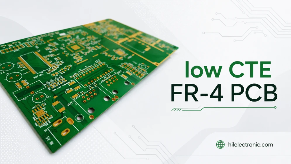
Low CTE FR-4 PCB Manufacturing for Through-Hole Reliability
Low CTE FR-4 PCB manufacturing is used when a circuit...
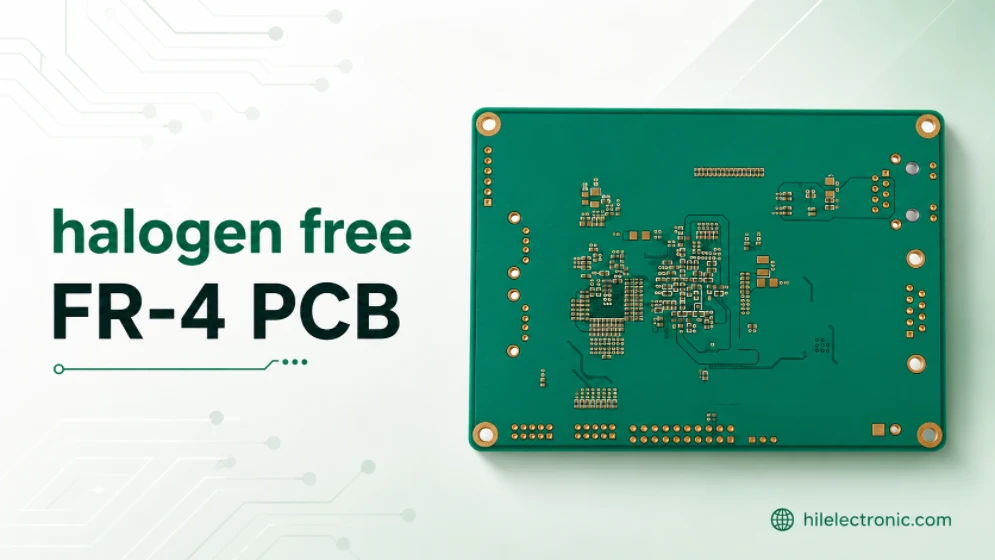
Halogen Free FR-4 PCB Manufacturing for Controlled Material Builds
Halogen free FR-4 PCB manufacturing is used when a product...
How to get a quote for PCBs
Let‘s run DFM/DFA analysis for you and get back to you with a report. You can upload your files securely through our website. We require the following information in order to give you a quote:
-
- Gerber, ODB++, or .pcb, spec.
- BOM list if you require assembly
- Quantity
- Turn time
In addition to PCB manufacturing, we offer a comprehensive range of electronic services, including PCB design, PCBA, and turnkey solutions. Whether you need help with prototyping, design verification, component sourcing, or mass production, we provide end-to-end support to ensure your project’s success.
For PCBA services, please provide your BOM (Bill of Materials) and any specific assembly instructions. We also offer DFM/DFA analysis to optimize your designs for manufacturability and assembly, ensuring a smooth production process.