
Circuit Board Reverse Engineering Services

Why Choose Professional Circuit Board Reverse Engineering Services?
When your critical electronic systems rely on obsolete or discontinued PCBs, professional circuit board reverse engineering becomes essential for maintaining operational continuity. At Highleap Electronics, we understand the urgency and precision required for successful PCB reconstruction, which is why we’ve developed comprehensive circuit board reverse engineering solutions that eliminate the common pitfalls plaguing this industry.
Modern electronic systems require seamless integration between design analysis and PCB Design optimization to ensure successful circuit board reverse engineering outcomes. Circuit board reverse engineering that rebuilds schematics, Gerbers, and BOM—multilayer/HDI supported. Fast quote, NDA, production-ready files.
The Hidden Traps in Circuit Board Reverse Engineering — And How We Avoid Them
Many companies in the circuit board reverse engineering market operate with deceptive pricing models. They attract clients with unrealistically low initial quotes, only to introduce additional charges midway through the project. Even worse, some providers deliberately embed traps in delivered files if clients choose not to proceed with their manufacturing services. These practices damage trust and can compromise your entire project timeline.
Highleap Electronics operates differently. Our transparent pricing structure includes all aspects of the reverse engineering process upfront. Whether you choose our manufacturing services or take your files elsewhere, you receive complete, uncompromised documentation without any hidden limitations or deliberate errors.

Non-Destructive vs. Destructive Circuit Board Reverse Engineering Methods
Non-Destructive Analysis
Our preferred approach utilizes advanced imaging technologies and layer-by-layer analysis without damaging the original PCB. This method preserves your sample board while extracting complete design information, including:
- Copper trace routing and geometry
- Component placement and orientation
- Via structures and layer stackup
- Drill hole specifications
The extracted data seamlessly integrates with modern PCB Fabrication processes, ensuring manufacturability without costly redesigns.
Destructive Analysis
When non-destructive methods cannot provide sufficient detail for complex multilayer boards, we may recommend controlled layer removal. This process involves careful delamination to reveal internal layer structures, though it requires sacrificing the sample board.
Our Comprehensive Board Reverse Engineering Process
1. Initial Assessment
We begin by thoroughly evaluating your PCB sample to understand your specific project needs. Our experts assess the board’s complexity and provide a roadmap for the reverse engineering process, ensuring we select the most appropriate techniques and tools for accurate results.
2. Method Selection
Based on the complexity of your PCB, we choose the most effective analysis method. Whether it’s optical scanning, X-ray analysis, or other techniques, we ensure we have the right approach to capture all the intricate details of your design, ensuring no critical elements are missed.
3. Data Extraction
This stage involves systematically extracting all essential design elements, such as the PCB layout, traces, components, and interconnections. Using specialized software and hardware, we ensure precise data capture to rebuild an accurate digital replica of your PCB.
4. Design Reconstruction
Using the extracted data, we create accurate CAD files that mirror the original design. Our engineering team ensures that every aspect of the design—trace widths, component footprints, and layer stackups—matches the original PCB to maintain full functionality.
5. Verification
Before finalizing the design, we conduct a thorough review to ensure its accuracy and manufacturability. We check that the design adheres to all industry standards and is ready for fabrication, minimizing any potential issues during production.
Highleap Electronics Circuit Board Reverse Engineering Advantages
Quality Assurance and Complete File Integrity
Every PCB Clone project undergoes rigorous quality control. Our experienced engineers verify dimensional accuracy, electrical connectivity, and component specifications before file delivery. Unlike competitors who may compromise file quality as leverage for manufacturing contracts, we maintain absolute integrity in all deliverables. Whether you choose our manufacturing services or work with other providers, you receive complete, uncompromised documentation without any hidden limitations or deliberate errors.
Advanced Technology and Integrated Solutions
Complex reverse engineering projects often require understanding of complete system architectures. Our Schematic Extraction capabilities ensure that circuit functionality is fully documented alongside physical layout information. For projects requiring immediate production capabilities, our PCB Assembly services provide seamless transition from reverse engineering to manufacturing.
Beyond board reverse engineering, Highleap Electronics offers comprehensive solutions including PCB Reverse Engineering services and PCB Copy capabilities for complete design documentation needs.
Trusted Partnership and Comprehensive Support
When you choose Highleap Electronics for board reverse engineering, you’re selecting a partner committed to transparency, quality, and your project’s success. Our decades of experience in PCB manufacturing and assembly inform our reverse engineering approach, ensuring designs optimized for reliable production. Our Complete PCB Cloning Solutions integrate all aspects of reverse engineering into streamlined project delivery.
Contact us today to discuss your board reverse engineering requirements. Experience the difference of working with a company that puts your success first, without hidden agendas or compromise.

Related Articles
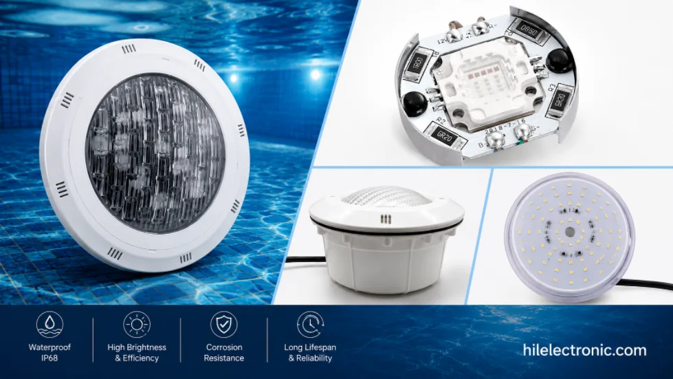
Underwater & Pool LED Light PCBs: IP68 Potted Boards, Low-Voltage Drivers & Safety
Figure 1. LED pool light PCB manufacturing reference....
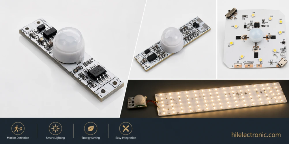
Motion Sensor & Smart LED Light PCBs: Sensor, Control, Driver & Wireless Boards
Figure 1. motion sensor LED light PCB manufacturing...

LED High Bay Light PCBs: Metal-Core Light Engines, Drivers & Turnkey Boards Built to Spec
Figure 1. LED high bay light PCB manufacturing reference....
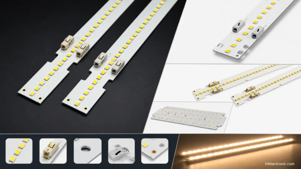
LED Linear & Strip Light PCBs: Long-Format Engines, Flexible & Rigid-Flex Boards
Figure 1. LED linear light PCB manufacturing reference....
How to get a quote for PCBs
Let us run DFM/DFA analysis for you and get back to you with a report.
You can upload your files securely through our website.
We require the following information in order to give you a quote:
-
- Gerber, ODB++, or .pcb, spec.
- BOM list if you require assembly
- Quantity
- Turn time
In addition to PCB manufacturing, we offer a comprehensive range of electronic services, including PCB design, PCBA (Printed Circuit Board Assembly), and turnkey solutions. Whether you need help with prototyping, design verification, component sourcing, or mass production, we provide end-to-end support to ensure your project’s success. For PCBA services, please provide your BOM (Bill of Materials) and any specific assembly instructions. We also offer DFM/DFA analysis to optimize your designs for manufacturability and assembly, ensuring a smooth production process.