
Power Inverter PCB Requirements for Solar, UPS, and Motor Drive Applications

Power inverter PCBs convert DC into AC for applications demanding everything from pure sine waves for sensitive medical equipment to rough square waves for simple motor control. The difference between a reliable inverter lasting 20 years on a rooftop solar installation versus one failing after months comes down to PCB design decisions made early in development.
How to Design H-Bridge PCB Layout for Solar Inverters
The H-bridge is where efficiency is won or lost in power inverter PCB designs. Every extra millimeter of trace length adds inductance, causing voltage overshoot and increased switching losses. We’ve seen 600V IGBTs fail in 400V systems due to layout-induced voltage spikes.
Key layout principles:
- DC bus capacitors must straddle the H-bridge with connections under 20mm
- Gate drivers position within 15mm of IGBT gates
- Current sensing in each leg for shoot-through protection
- Dedicated gate drive power supplies with isolated grounds
For a 10kW solar inverter, optimizing H-bridge layout improved efficiency from 96.5% to 97.8%—seemingly small but worth thousands in energy production over system lifetime. Similar optimization techniques apply to power electronics PCB designs across all power levels.
What Size DC Bus Capacitor for 10kW Inverter PCB
Above 5kW, traditional PCB traces can’t handle DC bus currents. Laminated bus bars provide ultra-low inductance but add cost and complexity. Our approach combines heavy copper PCBs with strategic bus bar integration only where absolutely necessary.
DC bus implementation strategies by power level:
- Under 3kW: 4-6oz copper planes on multilayer PCBs
- 3-10kW: Copper bus bars soldered to PCB pads
- 10-50kW: Laminated bus bars with integrated capacitors
- Above 50kW: Separate bus bar assemblies with PCB control boards
Film capacitors offer superior ripple current handling for DC bus applications. Position them symmetrically around the bridge for balanced current distribution. Add bleeder resistors for safety—a charged DC bus can kill. The same principles apply when designing high efficiency power PCB solutions for maximum performance.
Best Gate Driver Circuit for IGBT Inverter PCB Design
Isolated gate drives prevent catastrophic failures but require careful implementation. Optocouplers provide simple isolation but suffer temperature drift and aging. Digital isolators offer better performance but need proper power supply design.
Protection features that save inverters:
- Desaturation detection shuts down during short circuits
- Miller clamp prevents parasitic turn-on
- Soft shutdown reduces voltage stress during faults
- Active clamping limits voltage overshoot
For motor drive applications, implement hardware deadtime generation as backup to software control. We’ve seen software bugs cause shoot-through that hardware protection prevented. These protection strategies are equally important in power converter PCB designs handling similar power levels.
How to Calculate Output Filter for Pure Sine Wave Inverter
Pure sine wave inverters require LC output filters to remove switching frequency components. But output filters interact with inverter control loops, potentially causing instability. Size filter components for worst-case reactive loads, not just resistive ratings.
Filter design considerations:
- Inductor saturation at peak current including reactive loads
- Capacitor ripple current rating at switching frequency
- Damping networks to prevent resonance with load impedance
- Differential and common-mode filtering for EMI compliance
Grid-tie inverters need additional filtering to meet harmonic standards. LCL filters provide better attenuation than simple LC but require active damping. Our PCB assembly process includes network analyzer testing to verify filter response. Similar filtering techniques apply to power supply filter PCB designs.

Inverter PCB Thermal Design for -40°C to 70°C Operation
Solar inverters face temperature extremes from -40°C winter nights to 70°C internal temperatures on summer days. Component selection and PCB design must accommodate these extremes while maintaining 20+ year reliability.
Survival strategies for extreme environments:
- Use 105°C-rated capacitors minimum, 125°C preferred
- Implement conformal coating for humidity protection
- Design for natural convection—fans fail in dusty environments
- Position temperature-sensitive components in cooler zones
We helped a customer redesign their solar inverter for desert installation. Strategic component placement and improved thermal design eliminated premature failures plaguing the original design. These thermal management techniques also benefit power amplifier PCB applications operating in harsh conditions.
How to Reduce Noise in Inverter Control PCB
Modern inverters use DSP or microcontroller-based control requiring clean power and minimal noise coupling. Separate control boards from power stages when possible. When integrated, implement comprehensive isolation and shielding.
Control circuit best practices:
- Independent LDO regulators for analog and digital sections
- Multi-stage filtering on voltage/current feedback signals
- Differential routing for all sense signals
- Guard rings around sensitive analog circuits
For three-phase motor drive PCBs and variable frequency drives, encoder interfaces need special attention. Differential receivers and proper termination prevent position errors that cause motor control instability. Similar noise reduction techniques apply to DC-DC converter PCB control circuits.
Power Inverter PCB Testing Standards and Methods
Inverter testing must verify performance under real-world conditions, not just resistive loads. Test with motors, transformers, and non-linear loads matching actual applications. Verify stable operation with leading and lagging power factors.
Essential tests beyond basic functionality:
- Surge testing per IEC 61000-4-5
- Load step response with various load types
- Thermal cycling with power cycling
- Grid impedance variation for grid-tie inverters
Our electronic manufacturing service includes comprehensive inverter testing capabilities, from small UPS inverters to grid-scale power converters.
Choose Highleap Electronics for PCB fabrication that understands the unique demands of power inverter applications. We deliver robust solutions that survive harsh environments while maintaining peak efficiency.
Power Inverter PCB Design & Manufacturing FAQ
1. What is the difference between a solar inverter PCB and a UPS inverter PCB design?
Solar inverter PCBs emphasize MPPT interface integrity, high-voltage DC link management (typically 600–1100V), LCL grid filter control and anti-islanding compliance (e.g. UL 1741 / IEEE 1547). A UPS inverter PCB prioritizes fast transfer time, low total harmonic distortion (THD) under non-linear IT loads, battery management integration and short-term overload handling. Component derating, creepage/clearance and thermal cycling demands are typically harsher in rooftop solar vs indoor UPS. Many design principles—gate drive isolation, DC bus layout, EMI suppression—are shared across power electronics PCB platforms.
2. How is SiC inverter PCB layout different from IGBT inverter PCB layout?
SiC MOSFETs switch faster (high dv/dt & di/dt), making loop inductance and gate drive parasitics more critical. Gate loop & power loop separation, Kelvin source connections and ultra-short DC link capacitive loop (<10–15nH target) reduce overshoot and ringing. Gate resistance often becomes a tuning element for EMI vs switching loss. Common-mode current spikes require tighter shielding and proper Y-capacitor placement. Thermal density is higher; even with lower losses, junction-to-ambient gradients can concentrate without robust copper spreading. These considerations also enhance future-ready power amplifier PCB thermal stability.
3. How do I test inverter PCB reliability beyond basic functional checks?
Key layers: HALT/HASS (accelerated stress), thermal cycling with powered load, surge per IEC 61000‑4‑5, ESD per IEC 61000‑4‑2, conducted/radiated EMI pre-scan, partial discharge checks (≥800V), load profile replay (motor torque steps, grid impedance sweep), long-duration burn-in at elevated temperature. Data logging of switching energy, case temp gradients and fault counters improves predictive maintenance across solar, UPS and motor drive products within an integrated electronic manufacturing service workflow.
4. How to prevent IGBT or MOSFET shoot-through in inverter PCB layouts?
Combine: hardware interlock (deadtime logic), matched propagation gate drivers, tight gate loop routing, Miller clamp, proper gate resistors, desaturation / overcurrent sensing per leg and fast blanking management. Avoid long gate traces (>15–20mm) that introduce skew. For high-power motor drive PCB, include leg-by-leg current sensing to abort on asymmetry before full cross-conduction develops.
5. Can one inverter PCB support both grid-tie and off-grid (hybrid) operation?
Yes, but requires modular control: bidirectional DC link management, islanding detection (ROCOF / voltage phase shift), seamless transfer control, additional relay or solid-state transfer stage, adaptive output filter parameters and extended firmware safety state machine. Isolation monitoring and battery BMS interface must integrate early. Hybrid-ready architecture increases PCB layer count and test matrix, but reuses core power stage and gate driver design decisions from standard power converter PCB platforms.

Related Articles
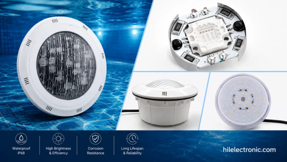
Underwater & Pool LED Light PCBs: IP68 Potted Boards, Low-Voltage Drivers & Safety
Figure 1. LED pool light PCB manufacturing reference....
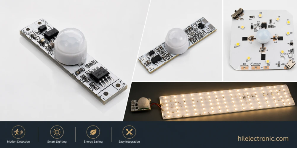
Motion Sensor & Smart LED Light PCBs: Sensor, Control, Driver & Wireless Boards
Figure 1. motion sensor LED light PCB manufacturing...
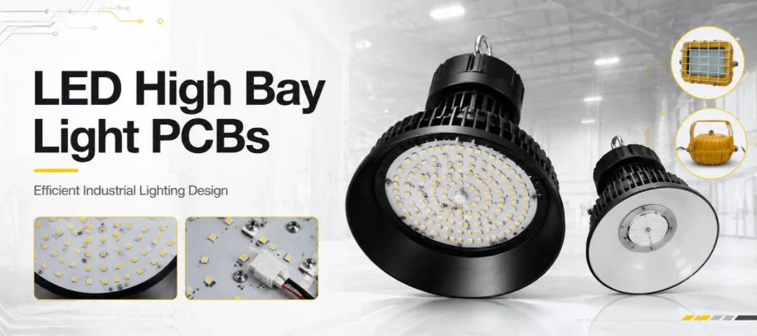
LED High Bay Light PCBs: Metal-Core Light Engines, Drivers & Turnkey Boards Built to Spec
Figure 1. LED high bay light PCB manufacturing reference....
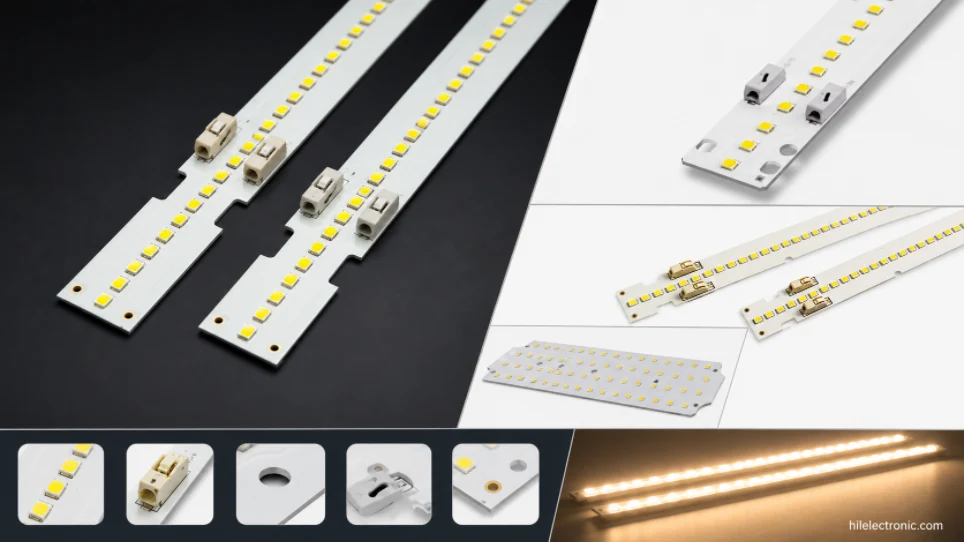
LED Linear & Strip Light PCBs: Long-Format Engines, Flexible & Rigid-Flex Boards
Figure 1. LED linear light PCB manufacturing reference....
How to get a quote for PCBs
Let us run DFM/DFA analysis for you and get back to you with a report.
You can upload your files securely through our website.
We require the following information in order to give you a quote:
-
- Gerber, ODB++, or .pcb, spec.
- BOM list if you require assembly
- Quantity
- Turn time
In addition to PCB manufacturing, we offer a comprehensive range of electronic services, including PCB design, PCBA (Printed Circuit Board Assembly), and turnkey solutions. Whether you need help with prototyping, design verification, component sourcing, or mass production, we provide end-to-end support to ensure your project’s success. For PCBA services, please provide your BOM (Bill of Materials) and any specific assembly instructions. We also offer DFM/DFA analysis to optimize your designs for manufacturability and assembly, ensuring a smooth production process.