
Stable Power Regulation PCB Solutions for Electronics

Power regulation PCB design determines whether sensitive circuits receive stable, noise-free power or suffer from dropouts, oscillations, and premature failure. From simple linear regulators to complex digital power management systems, proper PCB implementation makes the difference between specified and actual performance.
When to Use Linear vs Switching Regulator in PCB Design
Linear regulators seem simple but need careful layout for stability. Switching regulators offer efficiency but demand exceptional PCB design.
Linear regulator power regulation PCB essentials:
- Input/output capacitors within 10mm of regulator pins
- Adequate copper area for heat dissipation
- Kelvin sensing for remote voltage regulation
- Star grounding prevents ground loops
Switching regulator realities:
- Component placement determines efficiency and EMI
- Feedback routing requires noise immunity techniques
- Multiple ground planes need strategic connection
- Thermal management crucial despite high efficiency
For precision analog circuits, we often combine approaches: switching pre-regulator for efficiency followed by linear post-regulation for low noise. This hybrid approach also works well in Power Amplifier PCB power supply designs.
Power Supply Sequencing Circuit Design for FPGA
Modern systems require multiple voltage rails with specific sequencing requirements. FPGAs might need core voltage before I/O voltage. Analog circuits require symmetric rail tracking. Poor sequencing causes latch-up or component damage.
Sequencing implementation strategies:
- Dedicated sequencer ICs provide programmable delays
- RC networks offer simple but temperature-dependent timing
- Digital control enables complex conditional sequencing
- Fault handling must safely shutdown in reverse order
For complex power regulation PCB designs, we implement redundant sequencing verification. Similar sequencing challenges appear in Power Electronics PCB for motor control applications.
Point of Load Regulator PCB Layout Guidelines
Distributing high voltage and regulating at point-of-load improves efficiency and transient response. But POL regulators near sensitive circuits require careful integration to prevent noise injection.
- Switching frequency selection avoids interference with circuit operation
- Input filtering prevents conducted noise propagation
- Output capacitor selection balances transient response and stability
- Thermal coupling between regulators causes unexpected interactions
Recent processor designs use 20+ POL regulators. Our designs implement zone-based thermal management preventing cascading thermal failures. These multi-regulator strategies also apply to High Efficiency Power PCB systems.
How to Design DVS Circuit for Processor Power Supply
Modern processors vary voltage with workload for power optimization. PCB design significantly impacts transient response.
- Minimize output capacitance for faster voltage changes
- Position feedback networks for noise immunity
- Implement separate paths for AC and DC feedback
- Use differential remote sensing for accuracy
For mobile device DC-DC Converter PCB applications, DVS extends battery life by 30%.

LDO Capacitor Selection to Prevent Oscillation
Low-dropout regulators (LDOs) offer clean, low-noise power regulation, but capacitor selection is critical for stability. Incorrect ESR or layout choices can lead to oscillation and degraded performance.
- Verify ESR requirements — some LDOs need capacitors within a narrow ESR range for loop stability
- Add a small series resistor when using ultra-low ESR ceramic capacitors to prevent ringing
- Minimize PCB trace inductance in the output path to maintain phase margin
- Ensure proper thermal design for high-current LDOs to avoid thermal shutdown
Choosing the right capacitor network helps prevent oscillation and ensures reliable regulation. These stability principles also apply to Switch Mode Power Supply PCB control loop compensation, where component selection directly impacts EMI and efficiency.
PMBus Implementation in Server Power Supply PCB
PMBus enables digital power management with real-time telemetry, fault logging, and remote configuration—essential for data center reliability. Successful implementation requires careful hardware and PCB design.
- Use separate analog and digital ground planes, connected at a single point to avoid noise coupling
- Employ multi-stage filtering to provide clean, stable power for the digital controller
- Use galvanic isolation for PMBus communication when powering floating supplies
- Add watchdog and redundant protection to safeguard against firmware lockup
Proper PMBus integration allows remote monitoring, predictive maintenance, and better system uptime. These digital control techniques are equally valuable for Power Inverter PCB designs, enabling smarter fault diagnostics and improved power efficiency.
Power Supply PCB Load Transient Testing Methods
Thorough load transient testing is crucial to verify a power supply’s stability and performance under real-world stress conditions before mass production.
- Measure load step response across different slew rates to validate compensation design
- Introduce input voltage dips and surges to confirm ride-through capability
- Perform thermal cycling while under full load to reveal solder joint or component weaknesses
- Evaluate stability margins across temperature and component tolerance extremes
Our PCB assembly services integrate automated power rail testing, helping catch transient or stability issues early. This ensures every board meets performance standards before shipment.
Designing Scalable Power Regulation PCB for Future Upgrades
Design flexibility into power regulation PCB layouts for future modifications:
- Include footprints for optional components
- Plan for increased current requirements
- Consider migration to different regulator types
- Design test points for debugging and modification
These forward-thinking approaches benefit all power designs, from AC-DC Converter PCB to Power Converter PCB applications.
Trust Highleap Electronics for electronic manufacturing service and PCB fabrication that delivers reliable power regulation solutions.
FAQs
What is the typical layer count for Power Regulation PCB?
Most designs use 4–8 layers to separate power, ground, and signal planes, which improves EMI performance and current handling.
How do you minimize noise coupling in Power Regulation PCB?
Use solid ground planes, keep high di/dt loops as short as possible, and add RC filters for sensitive analog circuits.
What copper thickness is recommended for Power Regulation PCB?
Common designs use 2 oz copper for power layers to reduce IR drop, while signal layers can stay at 1 oz to control impedance.
How to ensure thermal reliability in Power Regulation PCB?
Implement thermal vias under power devices, optimize copper spreading, and simulate hotspot temperatures early in the design.
What testing methods validate Power Regulation PCB performance?
Perform load transient response tests, thermal cycling, EMI compliance checks, and ripple measurement before production release.
Can Power Regulation PCB be designed for modular upgrades?
Yes, using configurable footprints, jumper options, and extra test points allows future voltage/current scaling without redesigning the whole board.

Related Articles

Underwater & Pool LED Light PCBs: IP68 Potted Boards, Low-Voltage Drivers & Safety
Figure 1. LED pool light PCB manufacturing reference....
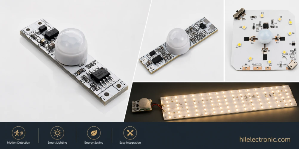
Motion Sensor & Smart LED Light PCBs: Sensor, Control, Driver & Wireless Boards
Figure 1. motion sensor LED light PCB manufacturing...

LED High Bay Light PCBs: Metal-Core Light Engines, Drivers & Turnkey Boards Built to Spec
Figure 1. LED high bay light PCB manufacturing reference....
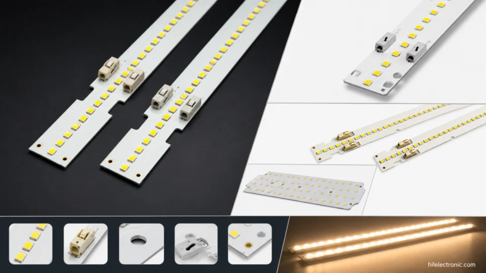
LED Linear & Strip Light PCBs: Long-Format Engines, Flexible & Rigid-Flex Boards
Figure 1. LED linear light PCB manufacturing reference....
How to get a quote for PCBs
Let us run DFM/DFA analysis for you and get back to you with a report.
You can upload your files securely through our website.
We require the following information in order to give you a quote:
-
- Gerber, ODB++, or .pcb, spec.
- BOM list if you require assembly
- Quantity
- Turn time
In addition to PCB manufacturing, we offer a comprehensive range of electronic services, including PCB design, PCBA (Printed Circuit Board Assembly), and turnkey solutions. Whether you need help with prototyping, design verification, component sourcing, or mass production, we provide end-to-end support to ensure your project’s success. For PCBA services, please provide your BOM (Bill of Materials) and any specific assembly instructions. We also offer DFM/DFA analysis to optimize your designs for manufacturability and assembly, ensuring a smooth production process.