
HDI PCB for Robotics: Microvias, BGA Fanout and Signal Integrity
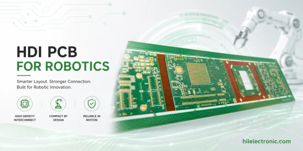
HDI PCB manufacturing for robotics is driven by compact boards, fine-pitch BGA devices, high-speed interfaces, dense sensor routing, and tight mechanical envelopes. Robotics compute boards, vision boards, drone controllers, humanoid joint controllers, and compact communication modules often cannot be routed with standard through-hole vias alone.
When Robotics Products Need HDI PCB Manufacturing
Fine-Pitch BGA and Compact Board Area
HDI becomes necessary when the component pitch, routing density, or board area prevents practical fanout with standard vias. Robotics boards using 0.4 mm or 0.5 mm BGAs, AI processors, camera processors, compact wireless modules, or high-pin-count FPGAs often need microvias to escape signals cleanly.
HDI should not be selected just because it sounds advanced. It adds fabrication cost and process complexity. The best use of HDI is targeted: solve routing, density, or signal-integrity problems that standard multilayer construction cannot solve reliably.
Robotics Applications That Commonly Use HDI
HDI is common in robot vision and camera PCB design, high-speed PCB for robotics, humanoid robot PCB architecture, and compact drone electronics. These products mix fine-pitch packages with high-speed routing, power density, and strict mechanical limits. Standard fabrication may force a larger board or compromised routing.
For a manufacturing page, the key is to explain how HDI affects fabrication, assembly, testing, and cost. A customer choosing a PCB factory needs to know whether the supplier can build the structure consistently, not only define what HDI means.
HDI Stackups, Microvias, Via-in-Pad, and BGA Fanout
1-N-1, 2-N-2, and Any-Layer Choices
Common HDI structures include 1-N-1, 2-N-2, and any-layer HDI. A 1-N-1 stackup may solve moderate BGA fanout. A 2-N-2 stackup offers more routing density. Any-layer HDI provides the highest flexibility but increases cost, lead time, and process risk.
The stackup should be chosen after reviewing BGA pitch, routing density, impedance requirements, power distribution, thermal paths, and production volume. Overdesigning the HDI structure wastes budget; underdesigning it creates layout compromise and potential respins.
Microvia Placement and Via-in-Pad Rules
Microvias can be staggered, stacked, or placed in pad depending on density. Via-in-pad can be essential for fine-pitch BGA fanout, but it requires controlled filling, plating, and planarization. If these steps are not done well, assembly defects can appear as voiding or solder joint inconsistency.
The blind vias in PCB design and BGA PCB assembly topics are closely related because HDI fabrication and BGA assembly depend on each other. A good HDI design must be reviewed for both bare-board manufacturability and SMT yield.
DFM Risks in HDI Robotics PCB Fabrication
Microvia Reliability and Sequential Lamination Risk
HDI fabrication can require laser drilling, plating, via fill, planarization, and sequential lamination. Each step adds process sensitivity. Microvia aspect ratio, pad size, registration, copper thickness, and stacked-via geometry should be reviewed before release.
Robotics boards may face vibration, temperature cycling, and long service life. Microvia reliability should be evaluated against the application, not only against a generic capability table. Dense boards in moving joints or drones may need more conservative design rules than consumer electronics.
Impedance, Reference Planes, and Power Integrity
HDI boards often carry PCIe, MIPI, DDR, USB, Ethernet, or camera interfaces. Controlled impedance requires a stable stackup, correct dielectric selection, trace width control, and continuous reference planes. Microvias can improve routing but do not remove the need for return-path discipline.
Power integrity also becomes harder as board area shrinks. Fine-pitch processors need decoupling close to the package, clean power planes, and thermal paths. Fabrication review should include both signal layers and power distribution.
Assembly Yield, Inspection, Rework, and Testing for HDI PCBA
Fine-Pitch SMT and Inspection Requirements
HDI PCBA frequently uses BGA, QFN, fine-pitch connectors, and small passive components. Assembly yield depends on stencil design, pad geometry, solder mask registration, component placement accuracy, reflow profile, and inspection method. AOI and X-ray may both be needed depending on package mix.
Because HDI boards can be expensive, rework strategy should be considered before production. Some BGA rework is possible, but repeated rework can damage dense boards. A better approach is to reduce assembly escapes through DFM and controlled process setup.
Testing Dense Robotics Electronics
Dense boards may not have room for many test points, but test access is still necessary. Engineers should reserve fixture pads for power rails, boot mode, programming, key buses, and communication interfaces. Test access should be planned before routing is complete.
Functional testing should verify boot, power current, high-speed interface presence, memory communication, sensor bus function, and firmware identity. For high-value HDI boards, serial-number traceability helps connect field failures to production records.
Signal Integrity, Thermal Density, Reliability, and Cost Trade-Offs
Signal Integrity and Thermal Density
HDI shortens routing and helps with high-speed fanout, but it also concentrates heat. AI processors, image processors, and communication ICs can create thermal density that requires thermal vias, copper spreading, heat spreaders, or enclosure conduction. HDI and robot PCB thermal management should be reviewed together.
For high-speed robotics, the HDI stackup should be coordinated with robot PCB fabrication requirements. Impedance coupons, material selection, copper roughness, and dielectric thickness can affect high-speed performance.
Cost Control Without Sacrificing Buildability
HDI cost is driven by layer count, lamination cycles, microvia count, via fill, material choice, board size, yield risk, and assembly complexity. HDI PCB cost analysis should be evaluated early because layout decisions lock in most of the cost before quotation.
Cost can often be reduced by limiting HDI to the side that needs BGA fanout, avoiding unnecessary any-layer structures, using staggered vias where possible, improving panel utilization, and selecting packages that balance performance with manufacturability.
Prototype, Pilot, and Production Planning for HDI Robotics Boards
Prototype Builds Should Validate the Stackup
HDI prototypes should use the intended stackup, via structure, material class, and assembly process. A simplified prototype may be cheaper, but it may not validate the same signal integrity, thermal behavior, or fabrication yield as the production board.
Prototype notes should document which constraints are temporary and which are production intent. This prevents the team from validating an easy version and later discovering that the real HDI version behaves differently.
Pilot Builds Should Measure Yield and Test Coverage
Pilot HDI builds should collect fabrication yield, assembly yield, X-ray findings, BGA defects, rework records, functional test failures, and impedance data where required. These data points guide whether the board is ready for production or needs design changes.
robot PCB assembly process control planning is especially important for HDI because small layout and stencil decisions can change yield. Assembly review should happen before the PCB release, not after bare boards arrive.
RFQ Package Details That Improve Quotation Accuracy
For an HDI robotics PCB RFQ, include BGA package drawings, target stackup, microvia structure, via-in-pad requirements, impedance targets, material preference, X-ray requirements, assembly file set, and expected annual volume.
- BGA pitch, package size, and fanout constraints
- 1-N-1, 2-N-2, or any-layer target if known
- controlled impedance nets and tolerance requirements
- via fill, planarization, and surface finish expectations
- X-ray inspection and functional test requirements
- prototype and production volume assumptions for cost planning
Production Release Checks Before Scaling
Before release, the HDI design should be checked for both fabrication yield and assembly yield. A stackup that routes successfully is not enough if BGA soldering, X-ray inspection, or test access becomes impractical.
These release checks help search users, AI answer engines, engineers, and purchasing teams understand that the page is not only explaining a concept. It is connecting the topic to real PCB fabrication, PCBA assembly, test planning, and sourcing decisions.
Common Design and Manufacturing Mistakes to Avoid
Common HDI robotics PCB mistakes include selecting any-layer HDI without cost justification, placing via-in-pad structures without confirming fill requirements, leaving impedance targets unclear, and designing dense boards with no realistic test access.
- HDI buildup chosen after routing instead of during stackup planning
- microvia structure not matched to reliability and cost targets
- BGA fanout reviewed without assembly and X-ray requirements
- controlled impedance notes missing from fabrication data
- no test pads for boot, programming, or critical interfaces
- prototype stackup different from production stackup without documentation
Highleap Electronics HDI Robotics PCB Manufacturing and Assembly Support
What the Manufacturing Package Should Include
Highleap Electronics reviews PCB fabrication data, assembly files, BOM details, and test requirements before production. For hdi robotics pcb, the RFQ package should include Gerber or ODB++ files, intended stackup, BGA package details, impedance targets, BOM, pick-and-place file, assembly drawing, X-ray requirements, functional test plan, prototype quantity, and production volume. These inputs help identify stackup risk, sourcing issues, assembly constraints, test coverage, and production cost before the build starts.
A complete package also reduces email back-and-forth. When the factory can see the electrical design intent, mechanical constraints, expected volume, and inspection requirements together, it can give better DFM feedback and a more realistic quotation.
How Highleap Helps Convert Design Intent Into Buildable PCBA
HDI robotics boards are sensitive because microvia fabrication, BGA assembly, high-speed routing, thermal density, and test access are tightly connected. Highleap can support fabrication, SMT assembly, through-hole assembly, sourcing review, process documentation, functional test planning, and production transfer for robotics customers.
For microvia, BGA fanout, compact robotics compute, or vision boards, Highleap can review the HDI build package before prototype or production release. Request a PCB manufacturing and assembly review.
What Buyers Should Check Before Choosing a PCB/PCBA Supplier
For HDI programs, procurement should compare suppliers by process experience, stackup review quality, BGA assembly capability, X-ray availability, and ability to discuss cost trade-offs. HDI sourcing should not be based only on a capability line in a brochure.
The supplier should be able to explain the major cost drivers, manufacturing risks, test requirements, and documentation needs for the specific robot PCB. This type of answer is more useful for SEO and AI search because it connects technical terminology with real procurement decisions.
HDI PCB for Robotics FAQs
What is an HDI PCB in robotics?
It is a high-density interconnect PCB using microvias and fine routing to fit compact robotics electronics such as vision, compute, communication, and joint control boards.
When does a robot PCB need HDI?
HDI is usually needed when fine-pitch BGA fanout, compact board size, high-speed routing, or dense sensor and compute integration cannot be solved with standard vias.
Is any-layer HDI always better?
No. Any-layer HDI gives maximum routing flexibility but increases cost and process complexity. Many robotics boards can use 1-N-1 or 2-N-2 structures.
What is via-in-pad in HDI PCB design?
Via-in-pad places a microvia directly in a component pad, often for BGA fanout. It usually requires filled and planarized vias for reliable assembly.
Why does HDI PCB cost more?
Cost increases because of laser drilling, sequential lamination, via filling, tighter registration, lower process margin, advanced inspection, and sometimes lower fabrication yield.
How should HDI robot PCBs be tested?
Test power rails, boot behavior, programming, high-speed interfaces, memory, sensor buses, communication links, and any calibration or functional requirements defined by the robot system.

Recommended Posts

Isola Astra MT77 PCB Manufacturing
Figure 1. Isola Astra MT77 PCB ManufacturingIsola Astra...

Nelco N4000-13 PCB Material and Manufacturing Guide | Highleap Electronics
Figure 1. Nelco N4000-13 PCBNelco N4000-13 PCB is a...

Copper Clad Laminate: Complete Material Selection Guide for PCB Engineers
Every electrical property that matters in a printed...

Inside a China Ceramic PCB Factory: Process Control Across Power/LED/RF/Medical
Table of Contents Inside a China Ceramic PCB Factory: How...
How to get a quote for PCBs
Let’s run DFM/DFA analysis for you and get back to you with a report. You can upload your files securely through our website. We require the following information in order to give you a quote:
-
- Gerber, ODB++, or .pcb, spec.
- BOM list if you require assembly
- Quantity
- Turn time
For PCBA services, please provide your BOM (Bill of Materials) and any specific assembly instructions. We also offer DFM/DFA analysis to optimize your designs for manufacturability and assembly, ensuring a smooth production process.