
Nelco N4000-13EP PCB Manufacturer for High-Reliability Multilayer Boards
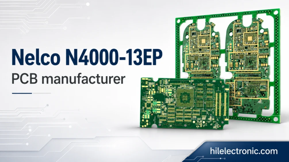
Nelco N4000-13EP PCB manufacturing is used for reliability-driven multilayer boards that require lead-free process compatibility, thermal stability, CAF resistance, plated-through-hole reliability, and repeatable production control. It is commonly selected for industrial control boards, communication equipment, embedded electronics, and multilayer assemblies exposed to multiple soldering or rework cycles.
Highleap supports N4000-13EP PCB projects through industrial PCB manufacturing, communication PCB manufacturing, multilayer PCB production, and reliability-focused DFM review. Before quotation, the stackup, material callout, IPC class, thermal exposure, via structure, assembly process, and inspection requirements should be confirmed.
N4000-13EP PCB Manufacturing for Industrial and Communication Electronics
N4000-13EP is selected when thermal reliability and lead-free process stability are important
N4000-13EP is suitable for multilayer PCB projects that need stable performance under lead-free assembly conditions. It is often used when standard FR4 may not provide enough thermal robustness, CAF resistance, or long-term reliability for the target application.
- Industrial control and embedded electronics
- Communication equipment and control modules
- Lead-free assembled multilayer PCBs
- Boards with repeated soldering or rework exposure
- Reliability-driven applications requiring stronger material control
Highleap reviews the expected operating environment, layer count, copper weight, via structure, connector density, surface finish, and assembly process before confirming the manufacturing path. These details help determine whether the requested N4000-13EP build can be produced consistently from prototype to batch production.
The fabrication drawing should clearly define the material callout, stackup, IPC class, finished thickness, copper weight, hole tolerance, surface finish, and required reliability documentation. A complete production package reduces material substitution risk, quotation uncertainty, and engineering holds before manufacturing.
N4000-13EP vs N4000-13EP SI: Reliability and Signal Integrity Boundaries
The article should separate reliability-driven builds from signal-integrity-driven builds
N4000-13EP and N4000-13EP SI should not be treated as the same manufacturing topic. N4000-13EP is mainly positioned around lead-free reliability, CAF resistance, thermal robustness, and multilayer fabrication control. N4000-13EP SI is more suitable when the project also requires SI glass, precise impedance control, and stronger signal-integrity focus.
- N4000-13EP: lead-free reliability, CAF resistance, and thermal robustness
- N4000-13EP SI: signal-integrity focus with SI glass and precise impedance control
- Different stackup review priorities for reliability-driven and SI-driven projects
- Material substitution approval required before production
For this reason, an N4000-13EP PCB manufacturing page should focus on manufacturability, thermal exposure, plated-hole reliability, lead-free assembly, documentation, and repeat production control. If the project is mainly about insertion loss, differential impedance, PCIe, Ethernet, or high-speed channel design, the material selection and stackup should be reviewed as a signal-integrity project.
N4000-13EP Lead-Free Multilayer PCB Stackup Design
Lead-free assembly exposure should be reviewed before the stackup is released
N4000-13EP projects are closely related to lead-free PCB manufacturing. The stackup should be reviewed for Tg, Td, thermal stress resistance, board thickness, copper balance, via reliability, and assembly temperature exposure before production.
Lead-free assembly can introduce higher thermal stress than traditional tin-lead assembly. For multilayer boards, this makes lamination quality, copper distribution, plated-through-hole reliability, and warpage control especially important.
- Layer count and dielectric structure
- Copper distribution and copper balance
- Finished board thickness and tolerance
- Lead-free reflow and rework exposure
- Via structure and plated-hole reliability
- Surface finish selected for assembly and storage needs
If the board includes BGA packages, large connectors, heavy copper areas, or asymmetric copper distribution, Highleap reviews warpage risk and thermal mass before production release. These checks help align the N4000-13EP stackup with both fabrication and assembly requirements.
CAF Resistance, Tg, Td, and Through-Hole Reliability
Material properties must be supported by correct board design and process control
N4000-13EP material data should be connected to the finished PCB construction. CAF resistance does not remove the need for proper conductor spacing, via field design, material cleanliness, and process control. High Tg and Td values also do not remove the need for balanced copper distribution, reliable plated-through holes, and controlled lead-free assembly exposure.
Highleap links reliability-driven material selection with PCB reliability review. For industrial boards, communication boards, and long-life embedded systems, the quotation package should define the required inspection level, documentation, and production controls before the purchase order is placed.
- CAF-sensitive spacing and via field review
- Cleanliness and process control requirements
- Through-hole reliability under thermal cycling
- Plated-hole quality and hole wall integrity
- Material lot traceability if required
- First article inspection notes if required
For reliability-critical boards, Tg, Td, CAF resistance, and through-hole reliability should not be treated as isolated material terms. They should be translated into fabrication notes, inspection requirements, and assembly controls that can be verified during production.
Fabrication Controls for N4000-13EP High-Reliability PCB
The board must survive fabrication, assembly, and long-term use conditions
Highleap treats N4000-13EP as a high-reliability multilayer PCB manufacturing topic. Lamination, drilling, desmear, plating, solder mask, surface finish, routing, electrical test, and final inspection should all match the reliability requirement.
The fabrication drawing should define IPC class, finished thickness, copper weight, minimum annular ring, finished hole tolerance, surface finish, electrical test method, and reporting requirement. If microsection, coupon, material certification, or first article inspection is required, these items should be listed before quotation.
- Lamination registration and thermal stress control
- Drilling quality and desmear process control
- Plating thickness and plated-through-hole reliability
- Solder mask adhesion and surface finish selection
- Electrical test and inspection requirements
- Microsection, coupon, or reliability report if specified
These controls affect cost and lead time because reliability requirements can change tooling, process monitoring, inspection coverage, documentation, and material purchasing. Clear production notes help Highleap confirm the correct manufacturing route before the quote is finalized.
N4000-13EP PCB Assembly, Inspection, and Traceability
Assembly and documentation requirements should be defined before production
N4000-13EP PCB projects often continue into assembly. If PCBA service is required, the production package should include BOM, pick-and-place file, assembly drawing, solder paste requirement, reflow restrictions, coating requirement, and test plan. These details help align PCB fabrication with the final assembly process.
For long-life industrial and communication products, traceability and inspection documentation may be part of the purchasing requirement. Highleap can review these needs during quotation so the required reports are included in the production plan instead of added after manufacturing has started.
- BOM and assembly drawing for PCBA projects
- Lead-free reflow profile limits if specified
- Rework and repair restrictions if required
- AOI, X-ray, ICT, FCT, or functional test requirements
- Material certificate and lot traceability if required
- First article inspection and production report requirements
To quote an N4000-13EP PCB accurately, Highleap needs Gerber, ODB++, or IPC-2581 files, fabrication drawing, stackup drawing, material callout, IPC class, copper weight, finished thickness, drill chart, surface finish, inspection notes, and assembly files if PCBA is required. A complete RFQ package allows the engineering team to review material availability, manufacturing risk, reliability requirements, documentation needs, cost, and lead time before production.
Submit the production package through the Highleap PCB quote form for stackup review, reliability check, and quotation.

Recommended Posts

Taconic RF-35 PCB Manufacturing Service — Prototype Through Volume Production
Figure 1. Taconic RF-35 PCBTaconic RF-35 is the workhorse...

Isola Astra MT77 PCB Manufacturing
Figure 1. Isola Astra MT77 PCB ManufacturingIsola Astra...

Custom Rogers RO4835 PCB Fabrication & Assembly Services
Figure 1. Rogers RO4835 PCBRogers RO4835 PCB is a...

Nelco N4000-13 PCB Material and Manufacturing Guide | Highleap Electronics
Figure 1. Nelco N4000-13 PCBNelco N4000-13 PCB is a...
How to get a quote for PCBs
Let’s run DFM/DFA analysis for you and get back to you with a report. You can upload your files securely through our website. We require the following information in order to give you a quote:
-
- Gerber, ODB++, or .pcb, spec.
- BOM list if you require assembly
- Quantity
- Turn time
For PCBA services, please provide your BOM (Bill of Materials) and any specific assembly instructions. We also offer DFM/DFA analysis to optimize your designs for manufacturability and assembly, ensuring a smooth production process.