
Nelco N4000-13SI PCB Manufacturer for High-Speed Signal Integrity Boards
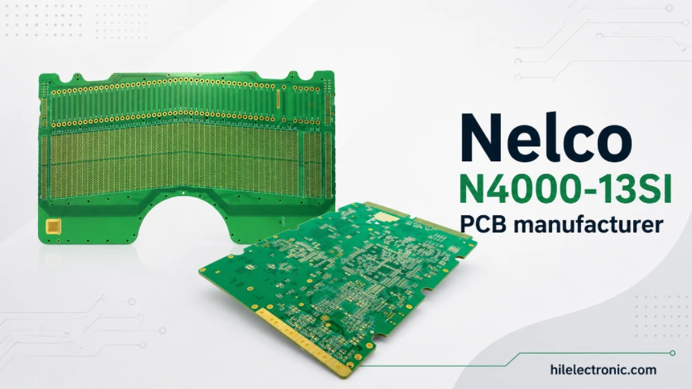
Nelco N4000-13SI PCB manufacturing is used for high-speed multilayer boards that require low-loss material performance, controlled impedance, stable registration, and repeatable fabrication. It is commonly selected for server boards, network switch boards, storage systems, FPGA carrier boards, communication modules, and backplane applications.
Highleap supports N4000-13SI PCB projects through high-speed PCB manufacturing, high-speed PCB material selection, controlled impedance production, backdrilling review, and high-layer-count PCB fabrication. Before quotation, the complete build package should be reviewed for stackup, impedance, via structure, BGA breakout, drilling, plating, surface finish, and inspection requirements.
N4000-13SI PCB Manufacturing for High-Speed Boards
N4000-13SI supports high-speed multilayer PCB production when the stackup and fabrication process are controlled together
N4000-13SI is suitable for PCB designs that need reliable signal integrity, precise impedance control, low signal loss, and stable thermal performance. In manufacturing, the material name alone is not enough to define the build. Highleap reviews the complete PCB construction before confirming production feasibility.
- Server and storage system PCBs
- Network switch and router boards
- FPGA carrier and communication control boards
- High-speed Ethernet and PCIe boards
- Backplane and connector-dense multilayer PCBs
- High-layer-count controlled impedance boards
The review usually includes layer count, material callout, dielectric thickness, copper weight, trace geometry, reference planes, BGA breakout, via structure, backdrilling requirement, impedance tolerance, and test coupon design. These factors affect signal quality, production yield, cost, and lead time.
For repeat production, Highleap also checks whether the same stackup can be held consistently from prototype to batch manufacturing. This is especially important for high-speed boards with tight impedance tolerance, dense BGA routing, or strict via stub limits.
N4000-13SI Low-Loss Stackup Planning
The material data should be converted into a manufacturable PCB stackup
N4000-13SI is selected for signal-integrity-oriented applications, but the final PCB performance depends on the actual stackup. Dielectric thickness, resin content, glass style, copper roughness, finished copper thickness, and reference plane structure all need to be considered during stackup planning.
Highleap can review the N4000-13SI stackup together with project requirements before CAM tooling. If the material has not been finalized, the engineering team can compare it with other high-speed PCB material selection options based on loss target, impedance requirement, availability, layer count, and production volume.
- Layer-by-layer material callout
- Dielectric thickness and tolerance
- Dk and Df values from the approved material data sheet
- Finished copper thickness and plating allowance
- Reference plane continuity
- Impedance coupon and test requirement
- Finished board thickness control
Small changes in dielectric height, copper thickness, etching compensation, or reference plane design can change the final impedance. For this reason, the stackup drawing and impedance table should be confirmed before production files are released.
Controlled Impedance PCB Fabrication with N4000-13SI
The impedance table should clearly define each controlled structure
N4000-13SI PCBs often include single-ended and differential impedance requirements. Highleap reviews trace width, spacing, layer position, reference plane, copper thickness, solder mask influence, and coupon design before manufacturing. This connects the signal integrity model with practical PCB impedance control.
A complete impedance table should not only list nominal values. It should define the signal layer, impedance type, target value, tolerance, trace width, spacing, reference layer, and measurement requirement. This avoids production ambiguity and helps the manufacturer confirm whether the design can be built within tolerance.
- Single-ended impedance by layer
- Differential impedance by layer
- Microstrip, stripline, or coplanar structures
- Trace width and spacing requirement
- Finished copper and etching compensation
- Coupon structure and measurement requirement
For high-speed boards, controlled impedance is not isolated from the rest of the fabrication process. Drilling, plating, copper balance, lamination thickness, solder mask, and surface finish can all affect the finished result. Highleap checks these items together before confirming the quotation and production plan.
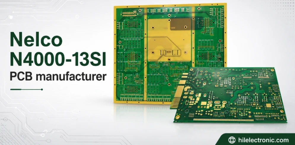
N4000-13SI PCB Stackup for PCIe, DDR, Ethernet, and FPGA Boards
High-speed interfaces require both suitable material and controlled fabrication
PCIe, DDR, Ethernet, and FPGA carrier boards require controlled return paths, stable impedance, length matching, crosstalk control, and clean layer transitions. N4000-13SI can support these applications, but the final result depends on stackup design, routing rules, via structure, connector breakout, and manufacturing control.
Highleap does not judge board performance from the material name alone. The project should provide layout rules, impedance targets, connector requirements, BGA information, backdrilling notes, and test expectations so the manufacturing plan can match the intended electrical performance.
- Differential pair routing and spacing
- Reference plane continuity
- Return path control near layer transitions
- Connector transition and escape region review
- BGA breakout density and layer-count impact
- Impedance and insertion-loss test requirements if specified
For dense PCIe, Ethernet, or FPGA boards, layer transitions should be reviewed together with via design. Poor via planning can introduce excessive stub length, impedance discontinuity, or routing congestion even when the selected laminate is suitable for high-speed use.
Via Stub, Backdrilling, and Layer Transition Control
Via structure is a major manufacturing factor in high-speed PCB performance
When N4000-13SI boards use high-speed connectors, dense BGAs, or long differential routes, via stubs can become a signal integrity risk. Highleap reviews whether standard through vias are acceptable or whether backdrilling, blind vias, buried vias, or HDI construction should be used.
If the board requires backdrilling, the fabrication drawing should define the backdrill side, target layer, residual stub requirement, depth tolerance, keep-out area, and inspection method. These details affect manufacturability, yield, and lead time, especially on high-layer-count boards.
- Backdrill depth and tolerance
- Allowed residual stub length
- Pad stack and annular ring requirement
- Connector breakout via design
- Blind and buried via feasibility
- Layer transition control for high-speed nets
If the project moves into HDI PCB manufacturing, the process path changes. Microvia structure, lamination sequence, via filling, copper plating, reliability testing, and cost should be reviewed before quotation.
BGA Breakout and HDI Options for N4000-13SI PCB
Component density can determine the final stackup and via strategy
High-speed boards are often limited by BGA pitch, fanout strategy, escape routing, and power distribution. N4000-13SI may be the selected material, but manufacturability still depends on via-in-pad design, microvia reliability, pad size, solder mask registration, layer count, and assembly yield.
Highleap reviews whether conventional through-hole fanout is enough or whether microvias, buried vias, via filling, or sequential lamination are required. The final build should support both signal integrity and assembly reliability.
- Fine-pitch BGA fanout
- Via-in-pad and filled via requirements
- Microvia and buried via structure
- Power and ground plane continuity
- Escape routing and layer-count planning
- Solder mask registration and assembly pad definition
For dense FPGA, processor, switch, or communication boards, BGA breakout should be reviewed before the stackup is frozen. A stackup that works electrically may still require adjustment if the escape routing, drill aspect ratio, or via structure is not manufacturable at the required yield.
Fabrication Controls for High-Layer-Count N4000-13SI Boards
High-layer-count boards require stable lamination, drilling, plating, and inspection control
N4000-13SI boards may be used in complex multilayer constructions where registration, copper balance, drilling accuracy, plating uniformity, and finished thickness control are critical. Highleap reviews these process factors before confirming production feasibility.
- Lamination sequence and press control
- Layer registration and scaling compensation
- Drill aspect ratio and hole wall quality
- Plating thickness and via reliability
- Copper balance and panel layout
- Bow, twist, and finished thickness control
- AOI, electrical test, impedance test, and cross-section inspection if required
For high-speed multilayer boards, fabrication controls should be written into the production documentation when they are critical to the design. This may include impedance reporting, backdrill inspection, cross-section reports, material certification, first article inspection, or other customer-specific requirements.
N4000-13SI PCB Quote Requirements and FAQs
A complete RFQ package allows accurate stackup review and quotation
To quote an N4000-13SI PCB, Highleap needs more than Gerber files. The production package should include the fabrication drawing, stackup drawing, impedance table, drill chart, material requirement, surface finish, finished thickness, inspection requirements, and assembly files if PCBA service is needed.
- Gerber, ODB++, or IPC-2581 files
- Fabrication drawing
- Layer stackup drawing
- N4000-13SI material callout
- Copper weight and finished copper requirement
- Controlled impedance table and tolerance
- Drill chart and via structure notes
- Backdrilling requirement if applicable
- BGA package information if breakout review is needed
- Surface finish requirement
- Finished board thickness requirement
- Impedance report, test coupon, or special inspection requirement
- Assembly files if PCBA service is required
Submit the production package through the Highleap PCB quote form. Highleap can then review material availability, stackup feasibility, impedance control, via structure, backdrilling requirement, inspection level, cost, and lead time before confirming the quotation.
FAQs
Is N4000-13SI suitable for high-speed PCB manufacturing?
Yes. N4000-13SI is used for high-speed multilayer PCB applications that require low-loss material behavior, precise impedance control, and reliable fabrication.
Does N4000-13SI alone guarantee signal integrity performance?
No. Signal integrity depends on the complete design and manufacturing process, including stackup, impedance control, copper roughness, via structure, reference planes, connector transitions, and inspection requirements.
When should backdrilling be considered?
Backdrilling should be considered when via stubs may affect high-speed signal performance. The requirement should be clearly defined in the fabrication drawing before quotation.
Can N4000-13SI be used for BGA and FPGA boards?
Yes. It can be used for BGA-dense and FPGA-related boards, but the fanout strategy, via structure, layer count, and assembly requirements must be reviewed together.
What affects N4000-13SI PCB lead time?
Lead time depends on material availability, layer count, lamination complexity, impedance testing, backdrilling, HDI structure, inspection requirements, and whether assembly is included.
N4000-13SI Fabrication Controls for High-Layer-Count Boards
Repeatability matters more than one successful prototype
A prototype that passes a bench test is not the same as a repeatable production build. Highleap reviews lamination registration, copper distribution, drilling quality, plating, etching, solder mask, and panel design so the same controlled-impedance result can be repeated later.
High-layer-count constructions can also be supported through backplane PCB and multilayer manufacturing review when the board is connector-heavy or rack-system oriented.
- Lamination registration and material lot control
- Copper roughness and etch compensation
- Plated-hole quality and annular ring review
- Production records for repeat builds
For a production N4000-13SI high-speed board RFQ, requirement should be converted into drawing notes and supplier checks rather than left as background explanation. Highleap uses it to decide whether the project needs material confirmation, stackup adjustment, DFM feedback, special inspection, or assembly process review before the quote is finalized.
The same requirement also affects cost and lead time because loss budget, impedance tolerance, via stub length, BGA breakout, and backdrilling yield can change tooling effort, process control, test coverage, or material purchasing. Providing stackup, impedance table, drill chart, BGA package data, backdrill notes, and test expectations before quotation reduces back-and-forth and makes the first engineering response more useful.
In practical builds such as servers, network switches, storage systems, FPGA carriers, Ethernet boards, and backplanes, this requirement normally appears during the first DFM or sourcing discussion. The reason is simple: loss control, differential impedance, BGA fanout, backdrilling, and layer transition quality can change the recommended stackup, inspection plan, or assembly sequence before a purchase order is placed.
For repeat production, Highleap also checks whether the requirement can be held from pilot build to batch production. That means the production package should give Highleap complete manufacturing inputs, not only a material name or a partial drawing set.
N4000-13SI PCB Quote Requirements
High-speed RFQs need engineering data, not only Gerbers
To quote N4000-13SI accurately, Highleap needs Gerber or ODB++ data, stackup, material callout, impedance table, drill files, backdrill information, fabrication drawing, finished thickness, surface finish, annual volume, and assembly files if the board is supplied as PCBA. Use the Highleap quick quote form to send the full package.
The strongest RFQs include the SI-critical notes at the beginning: controlled impedance, backdrilling, BGA pitch, inspection reports, and any customer test requirements.
- Stackup and impedance table
- Backdrill and via structure requirements
- BGA and connector assembly notes
- Testing, serialization, and traceability requirements
Quote readiness is a manufacturing quality issue for a N4000-13SI high-speed board. When files are complete, Highleap can review material availability, stackup feasibility, assembly risk, inspection level, and volume pricing without guessing from incomplete Gerber data.
The most useful RFQs identify stackup, impedance table, drill chart, BGA package data, backdrill notes, and test expectations. When those details are missing, the quote may look simple but can hide later engineering questions, material substitution risk, or assembly delays.
For servers, network switches, storage systems, FPGA carriers, Ethernet boards, and backplanes, quote speed depends on how complete the technical package is. Highleap can usually respond more accurately when the RFQ includes stackup, drawings, assembly files, required reports, and expected volume rather than only a ZIP of Gerber files.
This is especially important when loss control, differential impedance, BGA fanout, backdrilling, and layer transition quality affects yield. If the requirement is unclear at quotation, it often returns later as an engineering hold, material substitution question, or assembly exception.

Recommended Posts

Taconic RF-35 PCB Manufacturing Service — Prototype Through Volume Production
Figure 1. Taconic RF-35 PCBTaconic RF-35 is the workhorse...

Isola Astra MT77 PCB Manufacturing
Figure 1. Isola Astra MT77 PCB ManufacturingIsola Astra...

Custom Rogers RO4835 PCB Fabrication & Assembly Services
Figure 1. Rogers RO4835 PCBRogers RO4835 PCB is a...

Nelco N4000-13 PCB Material and Manufacturing Guide | Highleap Electronics
Figure 1. Nelco N4000-13 PCBNelco N4000-13 PCB is a...
How to get a quote for PCBs
Let’s run DFM/DFA analysis for you and get back to you with a report. You can upload your files securely through our website. We require the following information in order to give you a quote:
-
- Gerber, ODB++, or .pcb, spec.
- BOM list if you require assembly
- Quantity
- Turn time
For PCBA services, please provide your BOM (Bill of Materials) and any specific assembly instructions. We also offer DFM/DFA analysis to optimize your designs for manufacturability and assembly, ensuring a smooth production process.