
ITEQ IT-88GMW PCB for 77 GHz Radar Modules
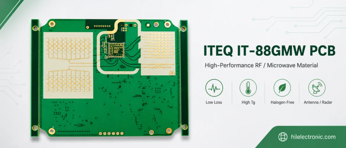
A 76–81 GHz automotive radar PCB is an electromagnetic structure, a mechanical datum, and a manufacturing process at the same time. The patch array, feed network, RFIC launch, ground fence, shield cavity, radome spacing, copper profile, dielectric thickness, and solder-mask boundary all participate in the final antenna response. For that reason, the laminate cannot be approved independently from the geometry that uses it.
ITEQ positions IT-88GMW as an ultra-low-loss, high-Tg RF laminate and prepreg family for long-, medium-, and short-range automotive radar in the 76–81 GHz band, as well as selected mmWave, antenna, microwave-link, and aerospace applications. Public ITEQ data list typical Dk 3.02 and Df 0.0013 at 10 GHz, Tg 185°C by TMA, T288 greater than 60 minutes, and stable dielectric behavior with temperature. Those figures identify the material class; they are not a license to enter 3.02 into a 77 GHz model without construction-specific correlation.
Why a 77 GHz Radar Board Cannot Be Treated as Scaled RF
At 77 GHz, the free-space wavelength is about 3.9 mm and the guided wavelength on a practical PCB is shorter. A dimensional error that is visually insignificant on a digital board can represent a meaningful fraction of a wavelength. The consequence is not limited to a small impedance change. It can move the resonance of a patch, alter the phase balance across an array, change the amplitude delivered to individual elements, increase cross-polarized radiation, or distort the beam.
This is why a radar board should not inherit the fabrication notes from a lower-frequency RF board. The critical dimensions include the finished dielectric thickness beneath the antenna, the etched top and bottom width of each feed line, copper sidewall slope, copper roughness, local resin content, glass-weave orientation, mask registration, cavity height, radome air gap, and package-to-line transition. The board drawing must distinguish which of these are ordinary mechanical dimensions and which are electrical characteristics.
| Variable | Why 77 GHz is sensitive | How to control it |
|---|---|---|
| Dielectric thickness under the radiating layer | It changes effective permittivity, line impedance, patch resonance, coupling, and phase velocity. | Freeze the exact core or cured prepreg construction; specify finished thickness and measurement method; correlate cross-sections to RF coupons. |
| Etched conductor geometry | Sidewall taper and over/under-etch change effective width and current distribution. | Use impedance artwork compensation, define copper weight and foil profile, inspect top/bottom widths on representative features. |
| Copper roughness | Skin-effect current follows the copper surface; roughness raises conductor loss and can alter phase. | Specify an approved VLP or equivalent foil by measurable profile and supplier construction, not only the phrase “low profile.” |
| Glass weave and resin distribution | Local Dk anisotropy can create phase imbalance and element-to-element variation. | Review glass style, trace orientation, resin content, spread-glass options, and panel orientation; validate on the released construction. |
| Solder mask and legend | Dielectric loading over a feed or antenna edge can detune the structure. | Create explicit keep-outs around patches, couplers, resonators, launches, and calibration features; control registration. |
| Shield, cavity, and radome spacing | Metal and dielectric objects near the antenna modify boundary conditions and radiation. | Model the actual housing and radome; define mechanical datums and tolerance stack; verify assembled modules. |
Tolerance is a performance allocation, not a generic capability
A fabricator may be capable of producing a narrow trace or a thin dielectric, yet the design can still be unreleasable if the allowed variation consumes the antenna-frequency or phase budget. The engineering team should allocate the permitted resonance shift, insertion-loss change, and phase error among material, etch, lamination, assembly, housing, and temperature. Only then can the supplier convert system targets into shop-floor controls.
For example, a patch length tolerance should not be selected from a standard line-width table. It should be derived from electromagnetic sensitivity analysis: sweep the patch dimensions, dielectric thickness, Dk, copper thickness, and mask boundary; identify the variables that move the center frequency or beam most; then assign practical manufacturing limits to those variables. The same method should be used for branch-line dividers, series feeds, corporate feeds, transitions, and matching structures.
Start With the Radar Module Architecture
The material decision changes with the radar architecture. A compact single-chip module with antennas on the package has a different PCB role from a board-level patch array fed by an RFIC. Likewise, a cascaded multi-chip array, a separate antenna board connected to a digital control board, and an antenna-in-package design create different demands on layer count, hybrid bonding, connector launches, thermal paths, and calibration.
| Module architecture | Primary PCB risks | IT-88GMW decision focus |
|---|---|---|
| Board-level patch array with RFIC on the same PCB | Antenna dielectric tolerance, RFIC launch, feed-network phase balance, shield/radome coupling. | Use the exact antenna construction as the design object; control mask keep-outs, foil profile, lamination movement, and assembly datums. |
| Separate antenna and processing boards | Board-to-board or coax launch, mechanical alignment, connector repeatability, return-path continuity. | IT-88GMW may be concentrated in the antenna board; validate the interconnect and reference-plane transition as part of the channel. |
| Hybrid radar/digital multilayer | CTE and cure compatibility, warpage, resin flow, registration between RF and digital substructures. | Qualify the full hybrid stack; do not assume two individually proven materials will laminate together without dimensional or reliability changes. |
| Antenna-in-package or package-radiating solution | PCB may carry high-speed digital, power, and lower-frequency RF rather than the main radiator. | A dedicated 77 GHz board laminate may be unnecessary on all layers; select material from the actual PCB function. |
| Cascaded or distributed array | Longer coherent feed paths, multiple device launches, calibration complexity, larger panel area. | Prioritize phase repeatability, panel-scale dimensional control, copper profile, and temperature correlation. |
The stackup review should therefore begin with a block diagram that marks every 76–81 GHz path, every radiating layer, every transition to package or connector, and every mechanical object inside the antenna near field. Digital, power, and control requirements should then be added without compromising the RF reference planes or antenna aperture.
Build a Geometry Budget Before the Stackup
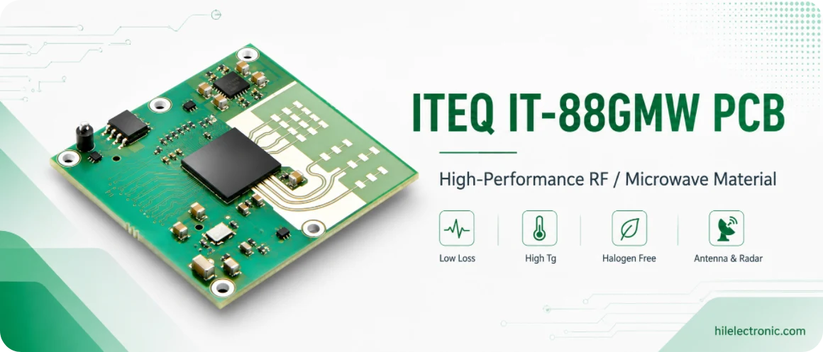
A useful release tool is a geometry budget. It turns “tight tolerance” into a list of dimensions, measurement locations, and acceptance evidence. The budget should be created before the final field-solver stackup because the solver needs realistic, producible ranges rather than ideal thicknesses.
- Freeze the functional RF layers. Identify the radiating surface, feed layers, ground references, package escape layers, and any stripline or microstrip transitions.
- Choose the glass style and resin-content range with the fabricator. Confirm which IT-88GMW cores and prepregs are routinely available, which can meet the target thickness, and which require special purchase.
- Specify copper by profile and finished thickness. Include base foil, plating contribution where applicable, treatment side, and whether rolled, reverse-treated, VLP, or another qualified profile is used.
- Model process variation. Sweep dielectric thickness, Dk, copper thickness, etch width, sidewall angle, solder-mask boundary, and housing spacing using the same geometry that production will build.
- Convert sensitivity into drawing limits. Mark critical-to-function dimensions and define the inspection or coupon that proves each one.
- Obtain a supplier stackup sign-off. The released impedance and antenna model should use the supplier’s proposed construction rather than a generic material library entry.
Keep the antenna construction simple where possible
Every additional ply, copper interface, bond layer, or hybrid transition introduces another tolerance and material interaction. A complex multilayer can be necessary for routing and integration, but the radiating layer should not become complicated without a clear benefit. Where the architecture permits, use a stable core beneath the antenna, keep the ground reference unbroken, avoid resin-rich local features that change the field distribution, and route noisy digital or switching-power structures away from sensitive aperture regions.
Copper balance and panel symmetry still matter. A board that meets local RF dimensions but warps after lamination or assembly can change the antenna-to-radome spacing and module sealing. The mechanical stackup should be reviewed together with the electromagnetic stackup, especially for large arrays, asymmetric shielding, thick copper, embedded metal, or a hybrid material build.
Antenna, Feed Network, Radome, and Cavity Co-Design
The antenna cannot be approved as an isolated artwork layer. The feed network sets amplitude and phase; the ground and via fence control return current and leakage; the package launch adds inductance and capacitance; the shield and cavity create nearby conductive boundaries; and the radome introduces dielectric loading. A material change can alter all of these relationships because the guided wavelength and field confinement change.
Patch and array review
- Use electromagnetic optimization on the finished copper geometry, including corner rounding, trapezoidal sidewalls, surface finish, and any solder-mask edge near the radiator.
- Check element-to-element spacing and feed phase across the full process window, not only at nominal Dk and thickness.
- Model the finite ground plane, board edge, mounting holes, screws, shields, housing ribs, connector bodies, and nearby metal that can disturb the aperture.
- Evaluate polarization purity, scan or beam shape, sidelobes, gain, efficiency, impedance bandwidth, and temperature shift on the assembled structure.
- Define panel orientation if warp/fill glass direction or artwork stretch could create a repeatable phase bias across the array.
Feed network and RFIC launch
The launch from the RFIC or package to the board is often one of the highest-sensitivity regions. Pad dimensions, solder-joint geometry, via-in-pad structure, antipads, ground vias, package escape, and reference-plane transitions should be simulated together. A laminate with low Df cannot compensate for a resonant via stub or a poorly returned signal current.
For a corporate feed, accumulated phase error can be more damaging than the loss of one short segment. For a series feed, RF impedance and radiation loading interact along the line. In both cases, line width, spacing, bends, tees, couplers, and element taps should be controlled as a coherent network. Do not apply a generic 50-ohm rule to every branch without considering the designed power division and element impedance.
Radome and module cavity
A radome is not merely a mechanical cover. Its dielectric constant, loss, wall thickness, curvature, paint, moisture, adhesive, air gap, and distance from the array can move resonance and change beam shape. The cavity or shield can also support parasitic modes or couple to the antenna edge. The mechanical drawing should therefore include the RF datum scheme that controls the antenna-to-radome and antenna-to-shield spacing.
Environmental validation should include the actual radome and housing, not an open-board substitute. Temperature, humidity, contamination, and mechanical stress may change the spacing or dielectric loading even when the bare PCB remains within specification.
Fabrication Controls That Matter at 76–81 GHz
At millimeter-wave frequencies, ordinary PCB inspection is necessary but not sufficient. AOI can find opens and shorts, yet it may not quantify copper sidewall shape, local dielectric thickness, foil profile, or mask loading at the places that dominate RF performance. The process plan should identify which characteristics are controlled by incoming material records, in-process metrology, coupon cross-sections, and final RF test.
| Manufacturing stage | Control item | Evidence to retain |
|---|---|---|
| Incoming material | Exact IT-88GMW laminate/prepreg grade, glass style, resin content, foil type, lot and shelf condition. | Certificate of conformance, lot traceability, current TDS, storage record, foil designation. |
| Imaging and etching | Critical line and patch dimensions, artwork compensation, panel position, top/bottom width, undercut. | Coupon measurements, microsection or dimensional metrology, process capability data for critical features. |
| Lamination | Finished dielectric thickness, resin flow, panel movement, registration, voids, cure, warpage. | Thickness map, registration coupons, press recipe, material temperature record, cross-sections, flatness data. |
| Drilling and via formation | RF ground-via diameter and position, via-wall quality, stub length, blind-via geometry. | X-ray/AOI, microsections, drill and plating records, backdrill depth measurement where used. |
| Solder mask and finish | Keep-out compliance, registration, thickness near RF structures, finish thickness and uniformity. | Mask registration report, visual/AOI record, surface-finish certificate and representative cross-section. |
| Final test | Continuity plus impedance, insertion loss, resonant frequency, or other agreed RF metrics. | TDR/S-parameter coupon data, antenna or module test report, serialized traceability. |
Etch compensation must match the actual copper stack
The artwork compensation for a thin VLP copper foil with little plating is not the same as the compensation for a thicker copper construction. Surface finish can also change the effective conductor geometry. The fabricator should release a process-specific finished-width target, and the designer should simulate the expected trapezoid rather than a perfect rectangle if the geometry is sensitive.
Mask keep-outs must be unambiguous
A note such as “no solder mask on RF” is too broad and too vague. Some RF lines may tolerate or intentionally use mask; patch edges, resonators, couplers, calibration standards, and launch regions may not. Define polygonal keep-outs in the fabrication data, state the registration requirement, and prevent legend ink from entering the same zones.
First-Article Coupons and Module-Level Validation
The first article should prove both the board process and the assembled radar function. A single impedance coupon is not enough because two boards can meet characteristic impedance while differing in insertion loss, phase, resonance, or antenna efficiency. Select coupons that isolate the dominant uncertainties in the released design.
| Coupon or test | What it demonstrates | Recommended use |
|---|---|---|
| Cross-section coupon | Finished dielectric thickness, copper thickness, sidewall profile, via quality, registration, bond integrity. | Place near representative RF geometry and at panel locations that reveal process variation. |
| TDR impedance coupon | Line impedance and discontinuity locations on the released layer construction. | Use the same copper, reference planes, line geometry, and process as the functional RF route. |
| Transmission-line S-parameter coupon | Insertion loss, return loss, phase, and lot-to-lot correlation over the relevant frequency range. | Include multiple lengths or de-embedding structures when practical; tie the result to material lot and panel position. |
| Resonator or material-correlation coupon | Effective dielectric behavior for the released construction and process. | Use to correlate the EM model; do not generalize the extracted value to unrelated constructions. |
| Antenna witness array | Frequency shift, gain/efficiency trend, element or array repeatability. | Useful during process qualification when direct module test is costly or obscured by electronics. |
| Assembled radar test | Final EIRP/receive behavior, beam pattern, calibration stability, environmental performance. | Use the production radome, shield, housing, RFIC assembly, and calibration procedure. |
At minimum, compare cold, room-temperature, and hot operation on representative modules if the application requires automotive temperature performance. The purpose is not only pass/fail; it is to correlate material and geometry measurements with the observed frequency, phase, and gain shifts. That correlation becomes the basis for future supplier changes and process-control limits.
What to do when the first article misses frequency
Do not immediately retune the patch artwork. First separate the possible causes: actual dielectric thickness, effective Dk, etched patch length, mask encroachment, surface finish, radome gap, cavity geometry, and calibration. Measure the built board and housing, update the model with as-built values, and identify whether the miss is systematic or random. A systematic model-to-hardware offset may justify a controlled design correction; random spread points to process capability or material-construction variation.
How to Write the IT-88GMW RFQ
A useful RFQ prevents the quotation team from replacing a frequency-specific construction with a familiar low-loss material that appears similar on a generic table. The request should tell the supplier which variables are frozen, which may be proposed, and what evidence is required before a substitution is accepted.
- Material identity: ITEQ IT-88GMW laminate and matching prepreg, exact construction or an explicitly approved equivalent.
- Application: 76–81 GHz radar antenna/feed board, including whether it is LRR, MRR, SRR, cascaded array, or hybrid digital/RF.
- Stackup: finished dielectric thicknesses, glass styles, resin content targets, copper weights, foil profile, plating contribution, and reference-plane assignment.
- Critical geometry: patch and feed dimensions, RFIC/connector launches, via-fence locations, cavity and board-edge datums, mask and legend keep-outs.
- Electrical controls: design Dk/Df source, impedance targets and tolerance, insertion-loss or resonator coupon requirement, frequency range, and de-embedding method.
- Mechanical controls: finished thickness, bow/twist, panel orientation, registration, warpage after assembly, and antenna-to-housing datum requirements.
- Process controls: lamination recipe qualification, etch capability, surface finish, drilling/backdrill, mask registration, storage, and lot traceability.
- First-article evidence: stackup report, material certificates, cross-sections, dimensional measurements, TDR/S-parameters, and agreed antenna or module results.
- Substitution rule: no material, foil, glass style, prepreg, or finish change without engineering review and correlation on the released test vehicle.
When IT-88GMW Is Not Enough—or Is More Than You Need
IT-88GMW is most compelling when the PCB carries the 76–81 GHz radiator or a loss- and phase-sensitive feed network and when the project benefits from a multilayer, modified-FR-4-compatible RF system. It may be more than necessary for a board that only carries low-speed control, power, or short digital interfaces. Conversely, the material name alone may be insufficient for an unusually narrow-band, high-gain, high-power, space, or tightly scanned array if the project requires dielectric data, thickness options, copper systems, or qualification evidence beyond what the proposed construction can support.
| Situation | Likely decision | Reason |
|---|---|---|
| Main PCB contains patch array and feed network at 76–81 GHz | IT-88GMW is a logical candidate, subject to construction and module qualification. | The material is explicitly positioned for automotive radar and supports low-loss multilayer RF structures. |
| PCB contains only radar processor, power, CAN/Ethernet, and low-frequency control | Use a reliability- or high-speed-digital material appropriate to those routes; IT-88GMW may not add value. | The radiating function is elsewhere, so the governing loss and tolerance requirements differ. |
| Very short 77 GHz transition on an antenna-in-package module | Evaluate whether the package and launch dominate; a dedicated full-board RF material may be unnecessary. | Material benefit depends on field distribution and path length. |
| Long coherent feed, large array, or stringent phase repeatability | Use IT-88GMW only with panel-scale dimensional, temperature, and phase validation; consider other specialized RF options if data or tolerance limits are insufficient. | The project may be controlled by phase stability, glass anisotropy, or mechanical integration rather than nominal Df. |
| Hybrid radar/digital board with many layers | Consider IT-88GMW on RF layers and another qualified material elsewhere, but qualify cure, CTE, flow, registration, and warpage. | A hybrid can optimize cost and function but adds process interactions. |
The correct stopping rule is evidence. If the released construction meets antenna efficiency, center-frequency, bandwidth, beam, phase, environmental, reliability, and manufacturing-yield targets with margin, a more exotic laminate is unnecessary. If it does not, changing material should be compared with changes to antenna topology, layer construction, foil, radome, housing, and process capability rather than treated as the only lever.
Common 77 GHz Release Mistakes
| Mistake | Why it fails | Better practice |
|---|---|---|
| Using the 10 GHz marketing Dk directly at 77 GHz | Frequency, test method, resin content, glass style, and construction affect the effective value. | Use construction-specific design data and correlate it with a released coupon or antenna test vehicle. |
| Calling every 50-ohm line equivalent | Launches, bends, tees, couplers, package pads, and radiating taps have different field structures. | Model the complete feed and transition geometry, not only straight-line impedance. |
| Allowing solder mask “per standard process” near the antenna | Mask thickness and registration can load sensitive edges or resonators. | Draw explicit keep-outs and inspect registration. |
| Specifying only laminate brand, not prepreg and foil | The actual dielectric and conductor behavior depends on the full material system. | Freeze core/prepreg construction, resin content, glass style, foil profile, and finished thickness. |
| Testing only bare-board continuity | A board can be electrically connected yet have unacceptable loss, phase, or resonance. | Add relevant TDR/S-parameter, resonator, antenna, and assembled-module tests. |
| Retuning artwork before measuring the first article | The frequency miss may come from thickness, mask, finish, radome, housing, or calibration. | Update the model with as-built measurements and identify the dominant cause first. |
A disciplined IT-88GMW project therefore looks less like a laminate purchase and more like a controlled radar-platform release. The material, geometry, process, enclosure, and validation plan are approved together, with enough traceability to explain both a passing build and a future deviation.
Manufacturer references and release notes
The ITEQ pages below support IT-88GMW’s radar-band positioning and the public typical properties cited in this guide. A production radar release should additionally obtain construction- and frequency-relevant design data from the laminate supplier and fabricator, then correlate those data with the selected coupon and module test vehicle.

Recommended Posts

Taconic RF 35 vs RO4350B PCB
Table of contentsRF-35 vs RO4350B Procurement and...

TMM4 Filter PCB Manufacturing
TMM4 filter PCB manufacturing is controlled by the...

TMM3 PCB Manufacturing for RF Modules
TMM3 PCB manufacturing is most useful where the RF module...

TMM6 PCB Fabrication
TMM6 fabrication is the process-control page for a mid-Dk...
How to get a quote for PCBs
Let’s run DFM/DFA analysis for you and get back to you with a report. You can upload your files securely through our website. We require the following information in order to give you a quote:
-
- Gerber, ODB++, or .pcb, spec.
- BOM list if you require assembly
- Quantity
- Turn time
For PCBA services, please provide your BOM (Bill of Materials) and any specific assembly instructions. We also offer DFM/DFA analysis to optimize your designs for manufacturability and assembly, ensuring a smooth production process.