
RO3203 PCB Manufacturing
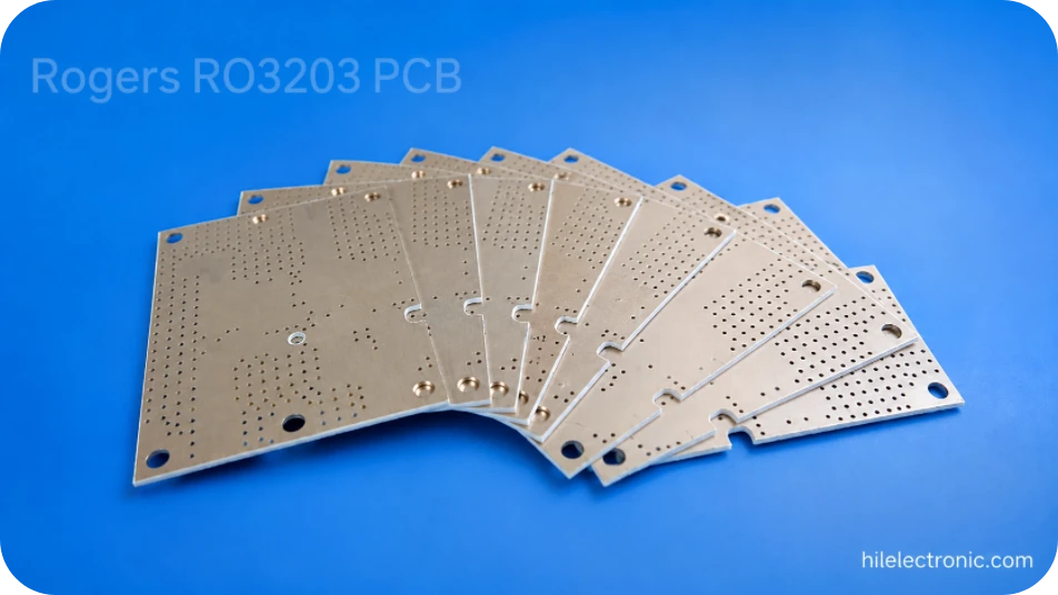
RO3203 PCB manufacturing for compact RF circuits depends on controlling the relationship between material thickness and small RF geometry. The design can benefit from a compact footprint only when those dimensions remain stable across the finished panel. RO3203 is the lowest-Dk member of the RO3200 series, but it is still a woven-glass-reinforced, ceramic-filled PTFE laminate rather than a generic compact-circuit material. Rogers publishes a process and design Dk of 3.02, a typical Df of 0.0016 at 10 GHz and a low published TCDk. The practical benefit is predictable low-loss geometry with greater rigidity than a non-woven PTFE sheet.
Highleap’s manufacturing objective is to preserve the customer’s RF intent: finished dielectric spacing, copper, line shape, mask boundaries, via grounding and any hybrid interface. The board should be released from critical finished dimensions and an acceptance method, not from artwork dimensions alone.
RO3203 production should be released from the RF geometry and finished dielectric construction. The manufacturing review focuses on dimensional consistency, copper definition, drilling and impedance verification for compact RF circuits.
Where RO3203 Creates a Practical Size Advantage
RO3203 can support compact distributed RF structures while avoiding the extreme geometry sensitivity associated with very high-Dk materials. It may be considered for filters, branch-line or directional couplers, impedance transformers, resonators, matching networks and selected antenna-feed sections. The value is not simply “smaller than low-Dk laminate.” The value is a workable balance among circuit dimensions, conductor width, bandwidth, loss and fabrication tolerance.
A design should begin with the electrical topology and the enclosure. If the product has enough area, a lower-Dk substrate may allow wider lines, lower local field concentration or broader bandwidth. If space is constrained, RO3203 may reduce the footprint while retaining more manufacturable geometry than a much higher-Dk choice. The correct decision comes from simulation using the manufacturer’s construction data and the intended copper, followed by prototype correlation.
| RF structure | Why RO3203 may be considered | Fabrication item to freeze |
|---|---|---|
| Compact filter | Reduces resonator dimensions without pushing immediately to the highest Dk tier. | Critical line/gap dimensions, finished dielectric and frequency target. |
| Coupler or divider | Supports controlled coupled-line geometry in a compact module. | Coupling gaps, copper thickness, registration and surface finish. |
| Matching network | Can shorten distributed matching sections. | Reference plane, line impedance and component pad transitions. |
| Antenna feed circuit | May suit compact feed or transition structures. | Mask keep-out, launch geometry and enclosure interface. |
| Hybrid RF/digital multilayer | Places RF functions on a dedicated layer while using another material elsewhere. | Bonding system, CTE compatibility, stackup and press qualification. |
Does higher Dk always improve an RF design?
No. Higher Dk reduces wavelength and physical size, but it can narrow traces, increase sensitivity to thickness and etching, concentrate fields and alter radiation efficiency. RO3203 should be selected because its properties fit the circuit, not because “high-Dk” sounds more advanced. The useful comparison includes electrical performance, producible line width, material availability, panel utilisation and first-pass yield.
Is RO3203 automatically suitable for an antenna?
The substrate may be suitable for certain antenna or feed designs, but antenna efficiency, bandwidth and radiation pattern depend on geometry, copper, ground, radome, housing and assembly. Highleap can manufacture the approved pattern and control critical dimensions. Final radiated performance normally requires the assembled module and customer-defined test setup.
For design context, review RF PCB miniaturization techniques rather than treating the laminate as the only size-reduction tool.
Material scope: Highleap Electronics manufactures and assembles the finished PCB. The Rogers grade named on this page identifies the specified laminate; Highleap does not manufacture or sell Rogers laminates.
Design and Fabrication Must Be Solved Together on RO3203
RF simulation assumes a physical cross-section. Production converts that cross-section into etched copper and pressed or supplied dielectric. The drawing should identify the exact RO3203 thickness, copper cladding, finished copper expectation, critical RF features and surface finish. If a value is derived from simulation but can be adjusted during impedance engineering, mark it accordingly. If a coupling gap or resonator length must not change, classify it as a controlled dimension. Highleap reviews line width, spacing, reference-plane distance, drilling and registration as a combined manufacturing problem. The first-article plan should identify which dimensions need recorded evidence and which can remain under standard PCB tolerances. Exact material property values should be checked against the current supplier documentation for the specified grade and construction.
Finished dielectric thickness
Nominal laminate thickness and finished dielectric spacing are not always interpreted identically in a design model. Copper cladding, foil removal, bonding layers and hybrid press cycles affect the cross-section. For a single RF core, material tolerance may dominate. For a multilayer build, bondply pressing and copper topography also matter. Highleap confirms the quoted construction and returns a stackup for approval where pressing is involved.
Microstrip and stripline geometry
Microstrip fields interact with air, solder mask and nearby metal. Stripline depends strongly on dielectric spacing and reference-plane symmetry. The choice should follow the product layout and shielding strategy. Critical traces should be modelled with the intended surface finish and copper thickness. The site’s microstrip guidance for high-frequency PCBs can help clarify which manufacturing inputs belong in the solver.
Etch compensation and copper sidewalls
Fine RF geometry changes during imaging and etching. The CAM team may adjust artwork so the finished conductor reaches the approved dimension, but the customer should identify electrically sensitive features. Overly narrow gaps, acute corners and isolated copper shapes can produce yield or variation issues. A first article can be used to correlate finished dimensions with measured frequency response before volume tooling is frozen.
Surface finish and solder mask
Surface finish changes conductor thickness and surface condition. Solder mask changes the local dielectric environment. Antenna, resonator and coupling areas often require mask keep-outs, while component pads need an assembly-compatible finish. The fabrication drawing should show those boundaries. A blanket note such as “green mask both sides” can be inappropriate when the RF model assumed exposed copper.
Highleap checks these details using a focused RF PCB tolerance review. The goal is not to apply the tightest tolerance everywhere; it is to apply appropriate tolerances to the few features that control the circuit.
Can RO3203 be combined with FR-4?
A hybrid construction may reduce cost or integrate digital layers, but it introduces CTE, bonding, resin-flow, registration and warpage considerations. The proposed bonding material and press cycle must be qualified for the exact stackup. Highleap reviews copper balance, material thickness, bond-line requirements, hole structure and assembly temperature before confirming a hybrid build.
Ordering an RO3203 PCB Without Losing the Original RF Intent
A good RFQ makes the design intent visible. Provide Gerber or ODB++, mechanical drawings, the RF stackup, exact material, copper type, surface finish, critical-dimension list, mask keep-outs, via details and test requirements. If component assembly is required, include the BOM, centroid, assembly drawings and functional test procedure. Highleap can then quote the same construction the engineer simulated.
- exact Rogers grade, laminate thickness and copper cladding;
- critical RF line widths, gaps, lengths and tolerance;
- impedance table and reference layers where applicable;
- surface finish, solder-mask boundaries and controlled edge features;
- hybrid materials, bondply and finished stackup if multilayer;
- prototype quantity, production forecast and required inspection records;
- PCBA BOM, placement, test and packaging data.
Prototype schedules depend on material stock, thickness, copper and testing. Highleap can support Rogers PCB prototyping, but a special construction should not be advertised as prototype until stock is verified. The Rogers PCB prototype route can include first-article dimensional checks and an agreed coupon before volume release.
If Highleap also assembles the circuit, panel support, stencil design, RF component orientation, shield frames and connector launches are reviewed with the bare board. RF assembly may require controlled cleaning, X-ray, hand placement of special components or functional testing. See the practical RF PCB assembly challenges that should be considered before the final panel is approved.
Payment, export packaging and shipping options are confirmed in the quotation. Small prototypes can ship by international express; production lots can use agreed courier or freight services. After delivery, Highleap retains project and lot information so a dimensional, fabrication or assembly concern can be reviewed against the approved data.
A practical prototype may compare more than one geometry
For a new filter or matching network, the first panel can contain small controlled variants around the nominal geometry when the customer’s design plan permits it. This approach can reveal the sensitivity to etch and dielectric tolerance without changing materials. The variants must be deliberate and documented; a factory should should not alter the RF pattern on its own.
Highleap can keep the variants on one controlled construction and provide dimensional results. The customer then correlates response and selects the production artwork. This can be faster than ordering separate boards after each frequency measurement.
Mechanical details can detune a compact RF board
Mounting screws, plated edges, shields, metal housings and board-to-board connectors change fields and ground currents. The mechanical drawing should show their positions and any controlled distance to RF features. A board that matches simulation in free space may shift after installation if the enclosure was not represented.
When assembly is included, Highleap checks shield-frame footprints, connector height and fixture access. Functional RF test is quoted only when the fixture, calibration and limits are defined.
Production inspection should focus on sensitive features
AOI can inspect all copper, while dimensional measurement can focus on resonator lengths, coupling gaps and launches. Finished thickness and board outline are measured according to the drawing. Microsection is used where plated holes or hybrid bond lines create risk. This targeted plan provides stronger evidence than applying extreme tolerances to ordinary traces.
Supply and repeat-order planning
RO3203 thickness and copper availability can affect schedule. A forecast allows material planning and consistent construction. If a later order requires another sheet size or copper option, Highleap submits the revised stackup and any geometry impact for approval. Repeatability depends on controlling these changes, not only reusing the same Gerber file.
After-sales review for RF products
If a delivered board shows a frequency or assembly issue, Highleap compares the returned sample with critical dimensions, material lot, finish, assembly record and test fixture. The investigation should distinguish bare-board geometry from component, housing and calibration effects. Clear first-article data gives both parties a useful baseline.
How to define controlled dimensions without over-tolerancing the board
Mark resonator lengths, coupling gaps, feed widths, launch clearances and any mechanically coupled cavity dimensions. Ordinary routing, text and non-critical copper can use standard manufacturing tolerances. This reduces inspection burden and prevents a drawing from becoming contradictory. Highleap can return a marked DFM question when a dimension is both tightly controlled and subject to normal etch compensation.
Where a critical dimension is measured at final copper, define the measurement points and whether surface finish is included. A line with trapezoidal sidewalls can produce different values at the top and base. The RF model should use a realistic conductor shape rather than an ideal rectangle if sensitivity is high.
Via and grounding strategy should be included in the RF review
Ground vias, via fences and component grounds support return current and shielding. Their spacing and finished diameter affect inductance. Blindly adding more vias can reduce routing space or create resin and drilling complexity. The customer should supply the intended ground strategy; Highleap checks drill spacing, annular ring and plating.
For plated edge or cavity structures, the drawing should define which edges are metallised and how continuity is tested. Edge plating can affect panelisation and cost, so it must be part of the initial quotation.
Thermal and power considerations
RF power devices can create local heat. RO3203 material choice does not replace thermal design. Copper spreading, thermal vias, metal housings and assembly interface materials should be reviewed. If a heatsink presses on the board, flatness and component height become assembly acceptance items.
Quotation lead time and convenient ordering
A complete RFQ allows Highleap to confirm stock and return a stackup quickly. Payment method and currency are agreed in the quotation. For prototypes, international express and online tracking provide convenient delivery. Production orders can use scheduled releases and agreed freight. These commercial services are useful only after the technical construction is frozen.
Handling nonconforming RF boards
If a dimension or response is outside the agreed limit, Highleap reviews containment, affected quantity and process data. Rework is evaluated only when it does not damage the RF structure or violate the drawing. Replacement, sorting or corrective action is determined from the evidence. This process provides a practical quality is intended to support without claiming that every system-level issue is a bare-board defect.
Documentation for regulated or high-reliability products
Industrial, medical, aerospace and automotive-related customers may require more than a standard certificate of conformity. The RFQ can identify material certification, lot traceability, inspection reports, first-article records and customer-specific document formats. Highleap confirms which records are included before the order so documentation does not become a delivery delay.
The inspection package should remain proportional to the product. A simple laboratory prototype may need only material confirmation and dimensions, while a released module may require a controlled build record. Clear documentation supports quality without turning the article or quotation into excessive marketing.
Design files should preserve revision history
RF boards often change after prototype tuning. The customer should send a complete revision package rather than only a replacement copper layer. Highleap checks artwork, drawing, stackup and assembly files for consistent revision. This prevents an old mask layer or drill file from being combined with a new resonator pattern.
A signed first-article approval can identify the exact production revision. Repeat orders then reference that baseline, making delivery and after-sales investigation more reliable.
Material note: use the latest controlled Rogers data sheet and the exact RO3203 construction in the RF model. Typical material data are not finished-board is intended to support. For quotation, provide the released stackup, minimum RF feature, copper, board size and quantity. That information makes the manufacturing tolerance and tooling requirements visible before production.

Recommended Posts

TMM4 Filter PCB Manufacturing
TMM4 filter PCB manufacturing is controlled by the...

TMM3 PCB Manufacturing for RF Modules
TMM3 PCB manufacturing is most useful where the RF module...

TMM6 PCB Fabrication
TMM6 fabrication is the process-control page for a mid-Dk...

TMM10 PCB Manufacturing for Compact RF Designs
Table of contentsHow TMM10 Shrinks RF StructuresTMM10 vs...
How to get a quote for PCBs
Let’s run DFM/DFA analysis for you and get back to you with a report. You can upload your files securely through our website. We require the following information in order to give you a quote:
-
- Gerber, ODB++, or .pcb, spec.
- BOM list if you require assembly
- Quantity
- Turn time
For PCBA services, please provide your BOM (Bill of Materials) and any specific assembly instructions. We also offer DFM/DFA analysis to optimize your designs for manufacturability and assembly, ensuring a smooth production process.