
Rogers RO4835T PCB Manufacturer for Thin-Core RF Multilayer Boards

RO4835T is useful when the RF layer must move inside the multilayer stack without consuming the thickness of a conventional microwave core. The buying decision is therefore tied to board architecture: dense radio modules, phased-array feed networks, compact transceivers and high-layer RF boards that need thin controlled dielectrics, short vertical transitions and stable inner-layer routing.
Highleap Electronics manufactures RO4835T prototypes and production multilayers with thickness-specific stackup review, spread-glass control, bondply selection, registration compensation and optional assembly. Highleap Electronics focuses on the thin-core construction problem rather than repeating a general RF laminate explanation.
Why Thin RF Cores Matter in Multilayer PCB Design
A thin inner dielectric can reduce via length, place a reference plane close to a controlled stripline and allow RF layers to coexist with digital, power and control circuitry in the same board. It can also improve routing density in compact modules. These benefits are only real when the design uses the selected core thickness from the beginning; substituting a thin core late in layout can change impedance, coupling and copper geometry.
Thickness-specific electrical data
RO4835T data are published by nominal core thickness. The 2.5, 3, 4 and 5 mil constructions should not be treated as one interchangeable material. The exact core and copper code must be attached to the stackup, because the model, line width and lamination result depend on that construction.
| Thin-core decision | Design benefit | Manufacturing consequence |
|---|---|---|
| 2.5–3 mil core | Shortest transitions and dense inner routing | Highest sensitivity to copper, etch and handling |
| 4–5 mil core | More line-width margin with a still-compact stack | Different electrical data and total-thickness impact |
| Spread-glass reinforcement | More uniform dielectric environment for fine routing | Exact construction must remain controlled |
| Inner-layer RF placement | Shielded stripline and compact module architecture | Registration and lamination become primary yield drivers |
Why spread glass helps but does not remove process variation
A spread-glass construction can reduce abrupt local resin and glass differences compared with coarse weave. That supports fine RF routing, but it does not eliminate sensitivity to finished thickness, copper profile or artwork movement. The field solver should use the exact construction, and the first article should correlate the predicted response with the built stack.
For broader design context, see Highleap’s high-frequency PCB stackup guidance.
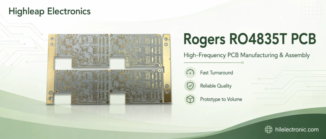
Manufacturing Thin RO4835T PCB Without Registration Issues
The main factory challenge is to keep a thin RF layer aligned and dimensionally stable through imaging, bonding and repeated thermal exposure. Inner-layer compensation, tooling strategy, copper balance and press sequence should be reviewed before panelization. A design with sequential lamination, blind vias or multiple thin RF cores needs a registration budget for every cycle, not one final outline tolerance.
Etch and copper decisions on thin layers
Thin dielectric spacing often produces narrow stripline geometry. Final copper thickness, sidewall shape and plating must therefore be included in the impedance model. The drawing should state whether the priority is finished line width, impedance or a critical coupling gap. Where a filter or coupler sits on an inner layer, direct inspection becomes more difficult after lamination, so inner-layer AOI and first-article records become more important.
- Freeze the exact thin-core thickness, copper and bondply before quoting.
- Review local resin demand around large clearances, dense vias and copper islands.
- Use inner-layer fiducials and compensation appropriate to the panel and press route.
- Define blind-via and sequential-lamination spans before selecting the bonding system.
- Retain first-article measurements for critical inner RF dimensions.
- Check total board warpage when thin RF cores are placed asymmetrically.
When the board uses more than one press cycle, Highleap reviews the construction against hybrid lamination and multilayer PCB manufacturing constraints rather than assuming a standard HDI route.
Where RO4835T Adds Value in Compact RF Products
RO4835T is strongest in products where a thin RF core changes the package architecture: phased-array modules, compact radios, inner-layer filters, dense antenna feeds and mixed-signal boards with shielded RF routing. It may add unnecessary complexity to a simple two-layer antenna board or a design that can use a standard RO4835 thickness without affecting enclosure size or via performance.
Thin internal stripline reduces board height and keeps RF routing shielded.
Controlled thin spacing supports compact phase routing and short transitions.
RO4835T can be reserved for selected internal layers while other materials carry digital and power functions.
A standard core may be easier to source and manufacture if the thin construction brings no architectural benefit.
First-article qualification
A useful RO4835T first article should prove the built thickness, inner-layer registration, critical line geometry, via quality and electrical response. If the board includes RF assembly, the correlation should extend to the assembled launch, connector or module. This evidence becomes the baseline for repeat production and change control.
RO4835T Stackup Review, Prototype and Production Support
The project package should include the exact core thickness, copper code, bonding layers, final board thickness, controlled impedance or RF geometry, via structure, lamination sequence and quantity. Material substitutions or changes to bondply should be submitted for approval because they can change the final dielectric spacing and resin distribution.
Highleap can provide prototype fabrication, low-volume production and repeat manufacturing, followed by component sourcing and PCB assembly where required. Lead time is confirmed after the thin-core construction and material stock are checked. For dense modules, the assembly plan should be reviewed together with the board because BGA escape, RF shielding, connector placement and reflow support can affect the multilayer architecture.
Send the intended RO4835T core thickness, full layer stack and via architecture. Highleap will review registration, bonding, impedance, sequential lamination and first-article evidence before production release.
Thin-core questions
Can RO4835T be substituted for standard RO4835 without redesign? Not automatically. The core thickness and published data are construction-specific.
Is the thinnest core always best? No. The electrical and packaging benefit must outweigh tighter etch, handling and registration tolerances.
Can RO4835T be used only on selected layers? Yes, provided the bonding system and full stack are qualified together.

Recommended Posts

Taconic RF-35 PCB Manufacturing Service — Prototype Through Volume Production
Figure 1. Taconic RF-35 PCBTaconic RF-35 is the workhorse...

Isola Astra MT77 PCB Manufacturing
Figure 1. Isola Astra MT77 PCB ManufacturingIsola Astra...

Custom Rogers RO4835 PCB Fabrication & Assembly Services
Figure 1. Rogers RO4835 PCBRogers RO4835 PCB is a...

Nelco N4000-13 PCB Material and Manufacturing Guide | Highleap Electronics
Figure 1. Nelco N4000-13 PCBNelco N4000-13 PCB is a...
How to get a quote for PCBs
Let’s run DFM/DFA analysis for you and get back to you with a report. You can upload your files securely through our website. We require the following information in order to give you a quote:
-
- Gerber, ODB++, or .pcb, spec.
- BOM list if you require assembly
- Quantity
- Turn time
For PCBA services, please provide your BOM (Bill of Materials) and any specific assembly instructions. We also offer DFM/DFA analysis to optimize your designs for manufacturability and assembly, ensuring a smooth production process.