
Rogers AD300D PCB Manufacturing for Low PIM
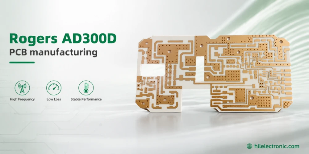
Rogers AD300D is a ceramic-filled PTFE antenna laminate with a Dk around 3.0, a typical loss tangent of 0.0021 at 10 GHz and published typical PIM performance of −159 dBc at 30 mil. It is used when an antenna or passive RF product needs controlled Dk, low loss, good power handling and a low-PIM material platform.
A low-PIM datasheet does not guarantee a low-PIM assembly. PIM is a system result created by material, copper, plating, solder, connector contact, mechanical pressure, contamination, fixture and test method. This article is organized around prevention and failure analysis rather than a generic PCB process.
Project review at a glance
| Best fit | Antenna and passive RF hardware needing a controlled Dk near three, low loss, power handling, and a low-PIM material platform. |
|---|---|
| Main manufacturing risk | PIM generated by plating, solder, connectors, dissimilar contacts, loose hardware, contamination, mechanical stress, fixture background, or inconsistent test conditions. |
| Expected engineering output | An AD300D fabrication, PCBA, mechanical, cleaning, and PIM-test plan with failure-analysis evidence tied to serial number or lot. |
What AD300D Brings to Low-PIM Antenna Hardware
AD300D provides a controlled Dk near 3.0, very good published PIM, larger panel availability and a thermal conductivity of 0.37 W/m·K at 100°C. Compared with lower-Dk antenna materials, it can reduce some feed and radiator dimensions while retaining a PTFE antenna-grade construction.
Rogers lists antenna, communication, power-amplifier and telematics applications for the AD Series. AD300D is compatible with standard PTFE fabrication, but the supplier must still control drilling, hole preparation, plating, etching, handling and cleanliness.
The AD300D process overview explains the material and fabrication issues, while our manufacturing capability summary covers supplier-selection questions.
AD300D vs AD250C: Dk, Size, and PIM Trade-Offs
| Decision factor | AD300D | AD250C | Selection implication |
|---|---|---|---|
| Dk | Approximately 3.0 | 2.50 ±0.04 | AD300D supports somewhat smaller RF structures; AD250C supports wider lines and larger radiators. |
| Typical Df | 0.0021 | 0.0014 | AD250C has the lower published dielectric-loss value. |
| Typical PIM | −159 dBc at 30 mil | −164 dBc | Both are low-PIM antenna materials; product-level PIM depends on the full assembly. |
| Design emphasis | Controlled Dk, broad antenna use, good power handling | Very low loss and strong published PIM performance | Choose according to size, loss, PIM, thickness, panel and supply needs. |
| Change control | Requires antenna re-simulation if substituted | Requires antenna re-simulation if substituted | Similar product family does not mean drop-in equivalence. |
For laminate selection, compare how candidate materials affect a low-PIM stack rather than choosing on Dk alone.
Applications: Small Cells, Outdoor Antennas, Microwave Links, and Telematics
| Product | Why AD300D may fit | PIM or manufacturing focus |
|---|---|---|
| Small-cell antennas | Compact passive RF structures and controlled Dk. | Connector density, shielding contacts and production test throughput. |
| Outdoor sector or panel antennas | Low-loss feed networks with good power handling. | Weather sealing, corrosion, grounding and mechanical contact. |
| Microwave-link antennas and feeds | Controlled electrical length and low-loss passive paths. | Launch geometry, radome interaction and alignment. |
| Telematics antennas | Compact antenna/feed integration across multiple bands. | Environmental cycling, cable strain and enclosure effects. |
| Passive RF distribution hardware | Low-PIM boards for dividers, combiners and feed networks. | Current path, joints, plating and hardware materials. |
Application constraints differ between antenna assemblies and RF power-amplifier hardware, even when both require low loss and stable RF performance.
Where Passive Intermodulation Is Created in a PCB Assembly
PIM is generated by nonlinear behavior in a passive current path. Common contributors include:
- ferromagnetic nickel, steel or contaminated metal in the RF path;
- loose or unstable connector and ground contacts;
- cracked, porous or incomplete solder joints;
- mixed-metal interfaces with corrosion or oxide films;
- flux residue, metal particles, fingerprints and process contamination;
- damaged plating or exposed base metal at edges and holes;
- mechanical movement under vibration, temperature or cable load;
- a test fixture, cable or adapter whose own PIM is close to the product limit.
A material certificate cannot detect these assembly-level sources. The design and process must treat every high-current contact as part of the PIM budget.
Process Controls for AD300D Fabrication
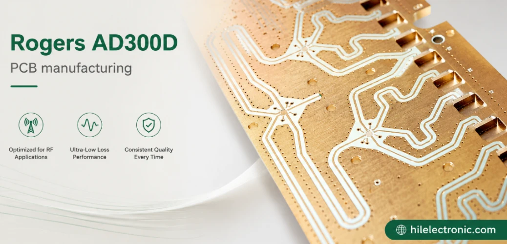
Fabrication controls should preserve the electrical and mechanical surface that the antenna design expects:
- confirm exact AD300D thickness, copper and material lot;
- use the approved PTFE drilling and hole-preparation route;
- control plated-hole copper and avoid residues that affect contact or reliability;
- apply etch compensation to the target finished RF geometry;
- protect low-profile copper and finished surfaces from scratches and embedded debris;
- define edge plating, exposed metal and grounding features clearly;
- inspect critical widths, gaps, board thickness and connector datums;
- package boards to prevent abrasion and contamination before assembly.
The fabrication plan should account for PTFE drilling, plating and dimensional behavior as well as the effect of finish selection on RF surfaces.
Connector, Solder, and Mechanical Assembly Controls
The connector launch should be treated as a controlled RF subassembly. Define connector manufacturer and plating, ground contact, solder volume, installation fixture, torque, cleaning, strain relief and visual criteria. Substituting a mechanically similar connector can change both RF response and PIM.
Highleap reviews stencil design and solder paste volume to avoid excess solder or incomplete joints. Mechanical screws, washers and shield contacts are checked against the approved material list. X-ray can verify hidden solder joints, but it does not replace PIM testing.
During assembly, plan for connector, solder and cleanliness risks and use X-ray where hidden joints need verification.
How to Build a Meaningful PIM Test Plan
| Test-plan item | What must be stated | Why it matters |
|---|---|---|
| Tone frequencies | Two transmit tones and intermodulation order. | The product response and interference band depend on the tone plan. |
| Power | Power per tone and allowed tolerance. | PIM level is sensitive to excitation power. |
| Limit | Acceptance value, units and measurement bandwidth. | A number without method cannot be compared. |
| Fixture | Cables, adapters, load, connector and product mounting. | Fixture PIM can mask or falsely fail the product. |
| Calibration/background | System residual PIM and verification method. | The test system needs margin below the product limit. |
| Mechanical state | Torque, cable position, enclosure and vibration condition. | Contact pressure and movement can change PIM. |
| Sampling | Prototype, first-article and production test quantity. | A single engineering sample does not define production control. |
Highleap can combine RF measurements at board or assembly level with functional checks on the finished product.
Troubleshooting an AD300D Assembly That Fails PIM
- Verify the test system: replace cables/adapters, measure residual PIM and confirm calibration.
- Repeat at controlled torque: connector or hardware pressure may reveal an unstable contact.
- Separate bare board and assembly variables: inspect surface damage, plating and contamination before replacing the laminate.
- Localize mechanical sensitivity: gently stress cable, connector, shield and mounting points under an approved diagnostic method.
- Review materials in the current path: connector plating, screws, washers, solder, finish and exposed metals.
- Clean and re-test: use the approved process; uncontrolled abrasion or chemical cleaning can create a new variable.
- Compare to a golden sample: physical and RF differences are more useful than repeating the same failed test.
- Document the root cause: update design, process, incoming inspection and production test—not only the failed unit.
Low-PIM Supplier Evaluation Checklist
- Can the supplier trace the exact AD300D lot and copper construction?
- Does it control PTFE drilling, hole preparation, plating and surface handling?
- Can it identify and exclude ferromagnetic materials in the RF path?
- Are connectors and mechanical hardware controlled by approved manufacturer and plating?
- Are soldering, cleaning and rework processes documented?
- Can the supplier measure critical RF geometry and connector position?
- Is the PIM fixture background verified below the product limit?
- Can it provide test data tied to serial number or production lot?
- Is there a documented failure-analysis and corrective-action process?
Use this low-PIM design review checklist during both design release and supplier evaluation.
Highleap Turnkey AD300D PCB Assembly Quote
Send Gerber/ODB++, drill, exact AD300D thickness and copper, stackup, critical dimensions, surface finish, BOM, approved component and connector list, assembly drawings, torque instructions, cleaning requirements and full PIM test plan.
Highleap can quote bare-board fabrication, component sourcing, PCB assembly, X-ray/AOI, mechanical integration and customer-defined PIM or functional testing. To receive an integrated response, send the Gerbers, BOM, assembly drawing and test limits.
Frequently Asked Questions
What can create PIM in an AD300D PCB assembly?
Potential sources include nonlinear metal contacts, poor plating, excess or cracked solder, loose connectors, ferromagnetic contamination, debris, dissimilar-metal interfaces, mechanical stress, cables, and fixtures.
How should a failed PIM assembly be troubleshot?
First verify the test system background and repeatability. Then isolate cables, connectors, torque, mechanical pressure, contamination, solder joints, plating interfaces, and board locations using a controlled change-and-retest sequence.
Can the material datasheet PIM value be used as the finished-product limit?
Not automatically. A laminate value is measured under defined conditions. The assembly limit, frequency, power, fixture, connectors, mechanical state, and acceptance method must be specified for the product.
What files are needed for an integrated AD300D quote?
Provide fabrication data, exact material and thickness, copper and finish, critical dimensions, BOM, approved connectors, assembly drawings, torque and cleaning requirements, and the full PIM or functional test plan.
Related Rogers PCB Manufacturing Resources
- Rogers TMM PCB Manufacturer & Assembly Supplier
- Rogers AD250C PCB for Low-PIM Antennas
- Rogers TMM PCB Price, Cost Drivers & Quote Guide
- Rogers TMM Aerospace PCB Supplier Qualification

Recommended Posts

Taconic RF-35 PCB Manufacturing Service — Prototype Through Volume Production
Figure 1. Taconic RF-35 PCBTaconic RF-35 is the workhorse...

Isola Astra MT77 PCB Manufacturing
Figure 1. Isola Astra MT77 PCB ManufacturingIsola Astra...

Custom Rogers RO4835 PCB Fabrication & Assembly Services
Figure 1. Rogers RO4835 PCBRogers RO4835 PCB is a...

Nelco N4000-13 PCB Material and Manufacturing Guide | Highleap Electronics
Figure 1. Nelco N4000-13 PCBNelco N4000-13 PCB is a...
How to get a quote for PCBs
Let’s run DFM/DFA analysis for you and get back to you with a report. You can upload your files securely through our website. We require the following information in order to give you a quote:
-
- Gerber, ODB++, or .pcb, spec.
- BOM list if you require assembly
- Quantity
- Turn time
For PCBA services, please provide your BOM (Bill of Materials) and any specific assembly instructions. We also offer DFM/DFA analysis to optimize your designs for manufacturability and assembly, ensuring a smooth production process.