
RO4003C Hybrid Multilayer PCB Manufacturing
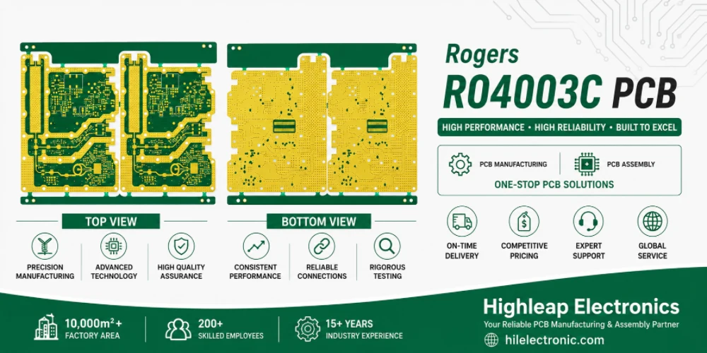
This page is the procurement and manufacturing entry for RO4003C RF and hybrid multilayer boards. It should answer how a specified RO4003C construction is converted into a manufacturable stackup and how the finished PCB is checked before repeat production.
RO4003C hybrid multilayer PCB manufacturing works when each material is assigned a clear electrical purpose in the stackup. The RF layers need controlled dielectric and conductor geometry, while FR4 sections can provide mechanical or cost advantages where the RF budget allows them. RO4003C is often the point where an RF project stops behaving like an ordinary FR-4 board. The change is not driven by the material name alone. It normally happens because insertion loss, phase consistency, filter response, antenna feed stability or production repeatability can no longer tolerate the spread associated with a general-purpose epoxy construction. The selected laminate construction should be carried into RO4003C fabrication controls, including drilling, bonding and finished-board verification.
Highleap Electronics supports RO4003C PCB fabrication from engineering samples through repeat production, including Rogers–FR-4 hybrid stackups, controlled impedance, plated through holes, selective solder-mask areas and optional PCB assembly. Highleap Electronics helps engineering and sourcing teams decide whether the upgrade is justified and whether the released stackup can actually be built repeatedly.
Material scope: This page concerns PCB fabrication using the specified Rogers material. Highleap Electronics manufactures the finished board and PCBA; laminate manufacturing and material sales are outside our service scope.
When Should Engineers Move From FR-4 to RO4003C PCB?
The strongest reason to move away from FR-4 is not frequency by itself. A short, tolerant RF trace may work on a carefully characterized FR-4 construction, while a narrowband filter or phase-matched feed network may require a controlled laminate at a lower nominal frequency. The decision should be tied to the electrical margin that disappears when dielectric thickness, Dk, copper profile and etch geometry vary across panels and production lots.
critical RF paths are short, loss margin is generous, phase tracking is not demanding and the product cost cannot justify a separate RF material.
filters, couplers, matching networks, antenna feeds or long transmission lines need lower loss and more predictable electrical length.
only a small number of layers carry RF energy while digital, power and control circuitry can remain on a lower-cost FR-4 system.
that changing the laminate automatically fixes connector launches, poor grounding, rough copper, uncontrolled mask or unsuitable via transitions.
What must remain consistent with the RF model?
Rogers publishes process and design dielectric values for RO4003C, but a production model still depends on the exact laminate thickness, copper foil, final copper, surface finish and local solder-mask condition. A quotation that specifies only “RO4003C” leaves too much room for interpretation. The fabrication drawing should identify the finished dielectric spacing under controlled RF traces and state whether line width or impedance is the governing acceptance criterion. Highleap reviews the transition between the material sets before lamination. Resin content, finished dielectric thickness, registration and copper balance all affect the finished multilayer geometry, so the hybrid stack should be released as a single construction. Exact material property values should be checked against the current supplier documentation for the specified grade and construction.
Copper roughness deserves particular attention. Once the dielectric loss is reduced, conductor loss can consume a larger share of the budget. The foil profile used in simulation should match the commercial construction that will be purchased. For compact filters or couplers, the finished line shape and gap can matter more than a generic 50-ohm coupon, so critical dimensions should be marked explicitly.
| Project symptom | What RO4003C may improve | What must still be controlled |
|---|---|---|
| FR-4 prototypes shift between lots | Tighter dielectric consistency and lower loss | Finished thickness, artwork compensation and copper profile |
| Long RF path consumes gain margin | Lower distributed dielectric loss | Connector, via and conductor-loss budget |
| Filter center frequency moves | More stable electrical length | Etched dimensions, housing, mask and assembly parasitics |
| Full Rogers construction is too expensive | Selective RF layers in a hybrid multilayer | Lamination compatibility, resin fill, registration and warpage |
For broader background on when a mixed construction is justified, see Highleap’s guide to FR-4 and Rogers PCB materials. The decision should be made before routing is frozen, because moving an RF layer later can change impedance, coupling and via geometry.

How Highleap Manufactures RO4003C Hybrid Stackup PCB
A hybrid multilayer is not simply an RO4003C sheet pressed onto an FR-4 board. The released construction must account for resin flow, copper distribution, cure behavior, dimensional movement and the location of RF reference planes. In many projects, the most stable route is to place the RO4003C core where its controlled dielectric thickness directly supports the RF layer, while bonding and support layers are selected to meet the total board thickness and reliability requirement.
Hybrid lamination and sequential build decisions
Some designs can be completed in one lamination cycle; others require sequential lamination because of blind vias, buried structures or separate RF subassemblies. Sequential lamination adds registration and cumulative thermal exposure. It should only be used where the interconnect architecture needs it. Highleap reviews copper balance, bondply fill, press sequence, drill spans and final thickness before the stackup is returned for approval.
- Freeze the exact RO4003C thickness and copper construction before impedance calculation.
- Define whether the bonding system is Rogers-compatible bondply, a qualified FR-4 prepreg or another approved material.
- Review local resin demand around heavy copper, large clearances and dense via fields.
- Use common mechanical and RF datums when antenna or filter geometry must align with a housing.
- Control drill entry, desmear and plated-hole preparation according to the mixed material stack.
- Specify solder-mask keep-outs around exposed RF structures instead of relying on factory defaults.
Registration is especially important when a thin RF core is placed inside a high-layer board. Inner-layer stretch compensation, imaging alignment and routing datums must be coordinated. The same applies to plated through holes: the hole passes through materials with different mechanical behavior, so drill quality, hole-wall preparation and copper thickness need to be evaluated as a complete interconnect.
Highleap’s hybrid PCB lamination process review is useful when the board combines RF laminate, standard FR-4, metal backing, cavities or multiple press cycles. For controlled transmission lines, the stackup is also checked against the project’s controlled impedance requirements rather than treated as a catalog construction.
A practical hybrid-board example
Consider a communication module with an RF front end, digital control, power conversion and board-to-board connectors. A full RO4003C build may add unnecessary cost and limit available prepreg constructions. A hybrid design can reserve RO4003C for the antenna feed, filter and amplifier matching layers while using a high-Tg FR-4 system for the digital and power sections. The result can be smaller material cost without moving the critical RF reference planes. For cost-sensitive designs, RO4003C and FR-4 application tradeoffs can help determine whether the RF requirement justifies a different material system.
The tradeoff is manufacturing complexity. The engineering package must define which layers are electrically critical, which dielectric gaps cannot be adjusted and where substitutions are prohibited. If the total thickness or copper distribution changes, the RF geometry may need to be recalculated instead of simply scaling the board.
RO4003C PCB Prototype and Production Considerations
Prototype quantities are valuable when the electrical response depends on several production variables at once. A useful first article does more than confirm continuity. It correlates finished dielectric thickness, line width, impedance or S-parameters, plated-hole quality and assembled RF behavior. This allows the design team to distinguish a laminate-model issue from an etch, launch, housing or assembly effect.
What should be reviewed before production release?
Instead of a generic RFQ checklist, Highleap uses an engineering review that focuses on the few variables capable of changing the released response. The normal input is Gerber or ODB++, stackup, material and copper callout, impedance table, critical RF dimensions, surface-finish requirements, solder-mask keep-outs, drill data, quantity and any required RF or mechanical inspection.
| Release item | Prototype evidence | Repeat-production control |
|---|---|---|
| RF dielectric spacing | Cross-section or thickness report | Approved stackup and material lot traceability |
| Critical line and gap geometry | First-article optical measurements | Etch compensation and in-process inspection |
| Impedance or insertion loss | Coupon or agreed RF measurement | Same coupon method and construction |
| Plated holes | Microsection and electrical test | Drill/desmear/plating process control |
| Assembly interface | Connector or module fit and RF correlation | Controlled stencil, reflow and inspection plan |
RO4003C boards can be supplied as bare PCBs or moved into component sourcing, SMT assembly, through-hole assembly and functional or RF testing where the required fixtures and limits are defined. For projects that need the complete build, Highleap’s PCB assembly services can be coordinated with the same material and stackup revision used for fabrication.
Lead time depends on the exact laminate thickness, copper construction, hybrid press route and quantity. prototype prototype production may be possible after material availability and the fabrication package are confirmed. Repeat orders benefit from frozen material substitutions, archived stackup data and lot-based production records.
Highleap engineers can review an RO4003C RF or hybrid multilayer stackup and identify material, lamination, impedance and assembly issues before the quotation is released. The goal is a construction that can be repeated, not merely a prototype that works once.
Common decision questions
Can RO4003C replace FR-4 without changing the layout? Usually not. Dk, dielectric spacing and copper assumptions differ, so line widths and resonant structures should be recalculated.
Can only one or two layers use RO4003C? Yes, a hybrid construction is often practical, but bonding, registration and reliability must be qualified as one stack.
Is a standard impedance coupon enough? It may be sufficient for transmission lines, but filters, couplers and antennas often require finished-dimension or RF-response correlation as well. For a hybrid quote, send the full layer stack, material locations, copper weights, target thickness, impedance requirements and quantity. This avoids quoting the RF section and the FR4 section as unrelated builds.

Recommended Posts

Taconic RF 35 vs RO4350B PCB
Table of contentsRF-35 vs RO4350B Procurement and...

TMM4 Filter PCB Manufacturing
TMM4 filter PCB manufacturing is controlled by the...

TMM3 PCB Manufacturing for RF Modules
TMM3 PCB manufacturing is most useful where the RF module...

TMM6 PCB Fabrication
TMM6 fabrication is the process-control page for a mid-Dk...
How to get a quote for PCBs
Let’s run DFM/DFA analysis for you and get back to you with a report. You can upload your files securely through our website. We require the following information in order to give you a quote:
-
- Gerber, ODB++, or .pcb, spec.
- BOM list if you require assembly
- Quantity
- Turn time
For PCBA services, please provide your BOM (Bill of Materials) and any specific assembly instructions. We also offer DFM/DFA analysis to optimize your designs for manufacturability and assembly, ensuring a smooth production process.