
China EV Charging PCB Manufacturing and Assembly

Highleap Electronics provides comprehensive PCB manufacturing and assembly solutions across automotive, industrial, telecommunications, and energy sectors. EV charging PCBs represent one of our most technically demanding specializations, where massive power handling meets automotive reliability standards. As electric vehicles transform transportation, we manufacture the charging infrastructure boards powering this revolution.
Heavy Copper EV Charging PCBs for High Current
EV charging PCBs must withstand extreme current demands far beyond conventional electronics. Ultra-fast chargers reaching 350kW can deliver more than 500 amps, which standard 1–2oz copper boards cannot support. To ensure safe and reliable operation, EV charging PCBs use
heavy copper PCB technology up to 10–20oz, enabling stable power delivery without overheating.
At Highleap Electronics, our EV charging PCB manufacturing process—built on advanced PCB fabrication expertise—ensures precise copper thickness control, optimized current distribution, and robust thermal vias. These techniques prevent hotspots and guarantee long-term durability, making our EV charging PCBs a dependable foundation for high-current charging systems.
Thermal Management in EV Charging PCBs
Thermal reliability is a defining factor in EV charging PCB design. Even at 95% efficiency, a 150kW DC fast charger generates several kilowatts of heat that must be dissipated continuously. Unlike consumer products, EV chargers run around the clock in outdoor environments from –40°C to +50°C.
We engineer EV charging PCBs with advanced thermal solutions including copper-filled vias, optimized via arrays, and optional metal-core substrates for superior heat conduction. For ultra-high-power chargers above 100kW, we integrate liquid cooling interfaces and temperature monitoring to ensure uninterrupted operation. These design strategies make our EV charging PCBs capable of handling continuous high-power loads with maximum reliability.
800V Architecture and Safety Requirements
Modern EVs use 800V batteries enabling faster charging with thinner cables. This voltage level demands exceptional attention to safety and isolation in PCB design.
IPC-2221 specifies minimum spacing, but we add 50% safety margin:
- Creepage distance: 15mm implemented (10mm minimum)
- Clearance through air: 12mm implemented (8mm minimum)
- Reinforced isolation: 8mm at 277VAC
- Physical slots between voltage domains
Isolation slots ensure safety even with contamination or component failure. We route 3mm slots between primary and secondary, maintaining strength with breakaway tabs during assembly. After population, tabs are removed leaving complete galvanic isolation.
Safety components require special attention. Y-capacitors bridge isolation for EMI suppression but must be safety-rated types. Optocouplers need 6mm keepout zones preventing creepage paths. Our power module PCB experience ensures comprehensive safety implementation.

Wide-Bandgap Semiconductors in Charging Applications
Silicon carbide (SiC) and gallium nitride (GaN) semiconductors enable unprecedented efficiency in EV charging, but their nanosecond switching speeds create new challenges.
At 50V/ns switching speeds, 2nH of parasitic inductance creates 100V overshoot—potentially destroying devices. We minimize parasitics through:
- Four-layer minimum with adjacent power/ground planes
- Vertical power loops through via arrays
- Kelvin source connections for gate drives
- Component placement minimizing loop area
Gate drive circuits require exceptional precision. Traces under 10mm length, matched impedance for timing accuracy, and isolated gate power preventing ground loops. These techniques refined through our GaN power PCB manufacturing ensure reliable wide-bandgap operation.
Communication Protocol Support
Modern EV chargers aren’t just power delivery—they’re intelligent systems communicating with vehicles, payment networks, and grid operators.
CHAdeMO and CCS protocols require high-speed CAN bus with controlled impedance, isolation crossing safety barriers, and robust ESD protection. Communication must continue despite kilowatts of power switching nearby.
OCPP backend connectivity enables remote monitoring through Ethernet with integrated magnetics, cellular modems requiring antenna isolation, and secure elements for payment processing. Our wireless charging PCB experience guides reliable communication integration.
Smart grid features including load balancing, renewable integration, and V2G capability demand sophisticated mixed-signal design. Digital sections need isolation from power circuits while maintaining reliable data exchange.
Frequently Asked Questions
Q: What are the main challenges in EV charging PCB design?
A: Primary challenges include managing 500+ amp currents, dissipating kilowatts of heat, maintaining 800-1000V isolation, and integrating communication protocols. Highleap Electronics addresses these through heavy copper processing up to 20oz, advanced thermal solutions, strict safety spacing, and mixed-signal expertise.
Q: What certifications are required for EV charging stations?
A: Key certifications include UL 2202/IEC 61851 for safety, FCC/CE for emissions, and regional requirements. Highleap Electronics designs ensure compliance through proper isolation, EMI control, and comprehensive documentation supporting certification.
Q: Can EV chargers work with renewable energy?
A: Yes, modern chargers integrate with solar, wind, and battery storage. Highleap Electronics manufactures PCBs supporting bidirectional power flow, grid-tie operation, and energy management systems through our AI data center power PCB grid interaction expertise.
Q: What’s the typical development time for EV charger PCBs?
A: At Highleap Electronics: prototypes in 5-7 days, typically 2-3 design iterations, and production-ready in 6-8 weeks. Our rapid prototyping using ultra-fast charging PCB techniques accelerates time-to-market significantly.

Related Articles
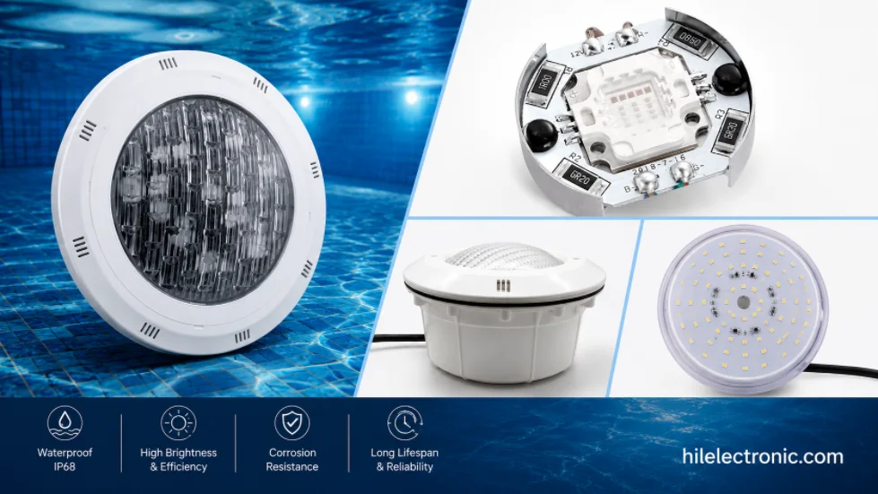
Underwater & Pool LED Light PCBs: IP68 Potted Boards, Low-Voltage Drivers & Safety
Figure 1. LED pool light PCB manufacturing reference....
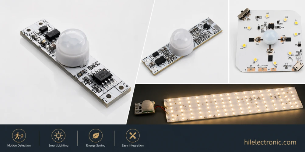
Motion Sensor & Smart LED Light PCBs: Sensor, Control, Driver & Wireless Boards
Figure 1. motion sensor LED light PCB manufacturing...
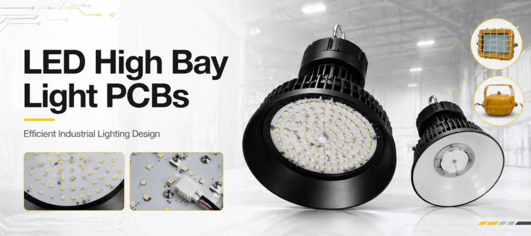
LED High Bay Light PCBs: Metal-Core Light Engines, Drivers & Turnkey Boards Built to Spec
Figure 1. LED high bay light PCB manufacturing reference....
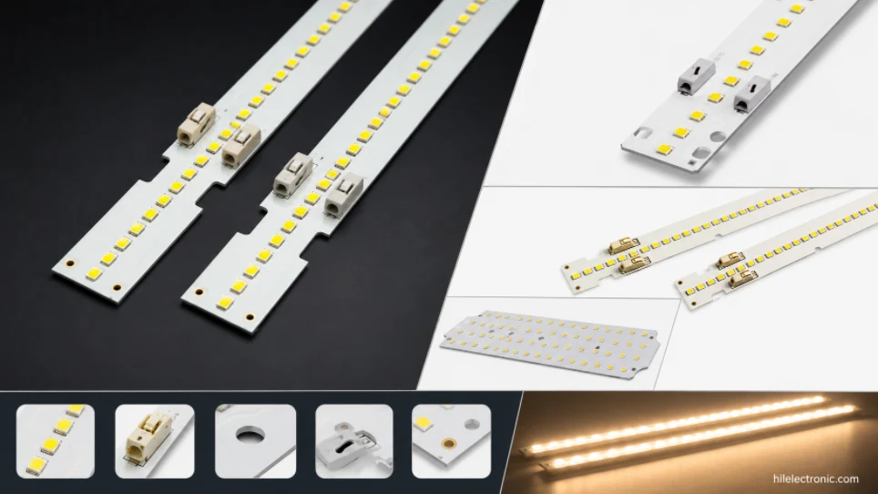
LED Linear & Strip Light PCBs: Long-Format Engines, Flexible & Rigid-Flex Boards
Figure 1. LED linear light PCB manufacturing reference....
How to get a quote for PCBs
Let us run DFM/DFA analysis for you and get back to you with a report.
You can upload your files securely through our website.
We require the following information in order to give you a quote:
-
- Gerber, ODB++, or .pcb, spec.
- BOM list if you require assembly
- Quantity
- Turn time
In addition to PCB manufacturing, we offer a comprehensive range of electronic services, including PCB design, PCBA (Printed Circuit Board Assembly), and turnkey solutions. Whether you need help with prototyping, design verification, component sourcing, or mass production, we provide end-to-end support to ensure your project’s success. For PCBA services, please provide your BOM (Bill of Materials) and any specific assembly instructions. We also offer DFM/DFA analysis to optimize your designs for manufacturability and assembly, ensuring a smooth production process.