
Glass PCB Applications in Electronics and Packaging

Glass PCB applications span multiple industries because glass can serve very different engineering roles depending on the product. In some designs, glass is selected because the circuit must remain transparent. In others, it is chosen because the substrate needs better dimensional stability, lower moisture absorption, stronger chemical resistance, or compatibility with package-style interconnection. This means glass PCBs are not defined by one single market. They are used across several application categories, each driven by a different technical requirement and a different production path.
At Highleap Electronics, glass PCB projects are usually reviewed from the application side first. A transparent LED panel, a package substrate, a biosensor platform, and an industrial glass circuit may all use glass, but they do not follow the same layout logic, interconnect structure, or manufacturing route. This is why understanding the actual application is the first step in determining whether a glass PCB is the right fit within broader glass PCB technology.
Discuss Your Glass PCB Application
Table of Contents
- RF Communication and Signal Platform Applications
- Advanced Semiconductor Packaging Applications
- Automotive and Mobility Applications
- Medical and Diagnostic Applications
- Transparent Display and Lighting Applications
- Industrial and Scientific Applications
- How to Match the Right Application to the Right Glass PCB Structure
- Glass PCB Applications FAQ
RF Communication and Signal Platform Applications
Glass PCB applications in communication hardware are usually connected to signal integrity, dielectric consistency, and compact substrate-level integration. These are not ordinary low-cost communication boards. They are more often signal platforms where the substrate has to remain electrically stable while also supporting fine routing, compact structures, or integration close to active devices.
Main RF-related application types
- Signal routing platforms: used where dimensional stability and consistent substrate behavior matter more than in ordinary laminate boards.
- Compact communication modules: used in tightly integrated systems where the substrate must support fine conductor geometry and stable circuit behavior.
- Package-level communication structures: used when the signal path is closely tied to package or interposer-style integration rather than to a standard board format.
In these projects, Highleap reviews whether the glass is serving as a board-level RF substrate, a signal redistribution platform, or part of a denser package-related structure. That distinction affects routing strategy, conductor type, stack-up planning, and whether the design overlaps with glass substrate selection or more advanced glass interposer structures.
Advanced Semiconductor Packaging Applications
Advanced packaging is one of the most important technical directions for glass PCB applications. In this area, glass is not chosen for transparency. It is chosen because package structures need flatness, dimensional stability, and better control of substrate behavior as routing becomes finer and package formats become larger or more integrated.
Main packaging-related application types
- Glass core package substrates: where glass serves as the structural core inside a package-level build.
- Glass interposer structures: where glass supports redistribution between finer die interconnect and the next package level below.
- Dense build-up platforms: where substrate-through interconnection and balanced structure become part of the package solution.
This application area is closely linked to glass core PCB, glass interposer, and through-glass via structures. At Highleap, these projects are evaluated as substrate engineering jobs rather than ordinary rigid PCB orders, because the manufacturing path depends heavily on interconnect density, build-up balance, and package function.
Automotive and Mobility Applications
Automotive glass PCB applications usually fall into two groups: functional electronic platforms and visible integrated glass products. Some are hidden inside sensing or control systems where stability and package compatibility matter. Others are visible parts of the vehicle interior where glass becomes both the circuit carrier and the finished design surface.
Typical automotive use cases
- Sensor-related assemblies: where glass supports compact electronic structures or optical access.
- Interior ambient lighting systems: where the glass panel itself becomes part of the visible lighting feature.
- Integrated mobility interfaces: where appearance, durability, and compact circuit integration have to be balanced.
For Highleap, automotive projects are reviewed for operating temperature, structural reliability, panel thickness, and whether the glass is part of the visible product surface. Applications involving interior illumination often connect naturally to LED glass PCB manufacturing, because those projects depend on both transparent appearance and stable LED circuit integration.
Medical and Diagnostic Applications
Medical and diagnostic products are one of the most natural matches for glass PCB technology because glass can combine optical access, chemical compatibility, electrical insulation, and fine structural control in one platform. In these applications, the substrate is often doing more than simply carrying a circuit. It may also be part of the sensing path, the fluidic path, or the imaging path.
Typical medical and biosensor use cases
- Lab-on-chip platforms: where the substrate may integrate sensing, heating, and fluidic functions.
- Optical biosensors: where the detection system must work through or on the glass surface.
- Diagnostic cartridges and imaging modules: where the circuit and optical structure must coexist in a compact space.
These applications often need careful control of optical zones, surface chemistry, and conductor compatibility. At Highleap, such projects are usually evaluated as functional glass platforms rather than standard transparent electronics, because the product requirement is usually tied to sensing or detection performance first.
Transparent Display and Lighting Applications
Transparent display and lighting is the most visible and commercially recognizable application category for glass PCBs. Here, the reason for using glass is straightforward: the circuit must work while the panel still looks transparent or visually open. An opaque laminate cannot deliver that result, so glass becomes both the substrate and part of the finished product appearance.
Main transparent application types
- Transparent display structures: where the product must remain see-through while still carrying an active circuit.
- LED glass lighting products: where the substrate supports visible lighting without becoming an opaque electronics panel.
- Decorative and architectural glass systems: where integrated lighting and product appearance matter equally.
This is the application area most closely associated with transparent PCB structures and LED glass PCB manufacturing. At Highleap, these projects are typically reviewed with separate visible-zone and support-zone logic so the center of the panel remains visually clean while connectors, bus structures, and denser routing stay near the perimeter.
Industrial and Scientific Applications
Industrial and scientific glass PCB applications are usually driven by stability, environmental resistance, optical compatibility, or long service life rather than by consumer-style appearance. In these applications, glass is selected because the substrate must remain reliable under demanding conditions or support precision structures over time.
Typical industrial and scientific use cases
- Precision instrument substrates: where dimensional consistency matters.
- Harsh-environment electronics: where moisture resistance and chemical stability are important.
- Scientific and calibration structures: where the substrate must support controlled measurement or optical-electrical interaction.
These projects often connect directly to glass PCB manufacturing decisions, because handling method, singulation, coating compatibility, and assembly route often determine whether the final product can meet the intended industrial or scientific requirement.
How to Match the Right Application to the Right Glass PCB Structure
The most effective way to evaluate a glass PCB project is to start with the role the substrate must play. A product that needs transparency should not be reviewed the same way as a package substrate. A diagnostic platform should not be treated like an illuminated architectural panel. Even when two products both use glass, their routing logic, conductor choice, interconnect structure, and assembly method can be completely different.
| Application area | Typical substrate role | Most relevant Highleap topic |
|---|---|---|
| RF communication | Signal platform or compact routing substrate | glass substrate selection |
| Advanced packaging | Core substrate or interposer platform | glass core PCB / glass interposer |
| Automotive | Sensor support or visible lighting substrate | LED glass PCB |
| Medical diagnostics | Functional optical-electrical platform | transparent circuit structures |
| Transparent lighting and display | Visible transparent circuit substrate | LED glass PCB manufacturing / transparent PCB |
| Industrial and scientific | Stable or harsh-environment substrate | glass PCB manufacturing |
At Highleap, application review usually starts with a few practical questions: Is the glass part of the visible product? Is it supporting package-style routing? Does it need substrate-through interconnection? Does it need special chemical or optical compatibility? Once those answers are clear, the right glass PCB structure becomes much easier to define.
Glass PCB Applications FAQ
Which glass PCB applications are the most commercially established?
The most established categories are transparent electronic structures, package-related glass substrates, visible glass lighting products, and industrial or sensor platforms where glass provides a clear functional advantage over standard laminate materials.
Can one glass PCB serve more than one function in the same product?
Yes. That is one of the main reasons glass is selected. A single glass substrate may support circuitry while also functioning as an optical window, visible design surface, sensor platform, or package-related structural element.
How do I know whether my project really needs a glass PCB?
The best starting point is to define the role of the substrate. If the project needs transparency, package-style flatness, special interconnect structure, sensing compatibility, or stronger environmental resistance, glass may be worth evaluating. If it only needs a conventional rigid board, standard laminate is usually more cost-effective. Highleap often reviews this question together with glass PCB vs FR-4 material selection.
What kinds of glass PCB projects does Highleap support most directly?
Highleap’s main support areas include transparent lighting panels, package-related glass substrates, interposer-type structures, industrial glass circuits, and application-specific glass PCB fabrication where the substrate role has already been clearly defined.
What should be submitted for application review?
The most useful starting information is the product type, substrate role, panel or substrate size, visible-area definition if relevant, whether substrate-through interconnect is required, and whether the project needs bare board fabrication only or full assembly support. These details can be submitted through the quote form for capability review.

Recommended Posts
LED Parking Lot Light PCB Manufacturing & Assembly by Highleap Electronics
Figure 1. LED parking lot light PCB production and...
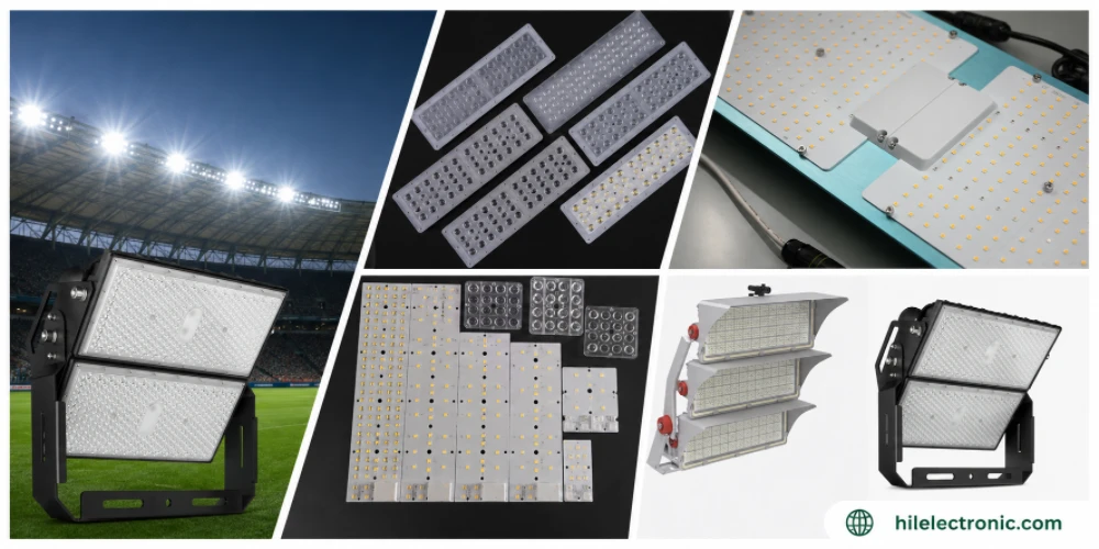
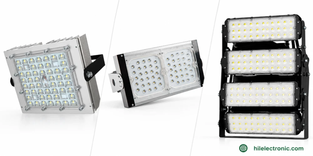
LED Stadium Light PCB Manufacturing — Very-High-Power Engines & Flicker-Free Drivers
Figure 1. LED stadium light PCB production and assembly...
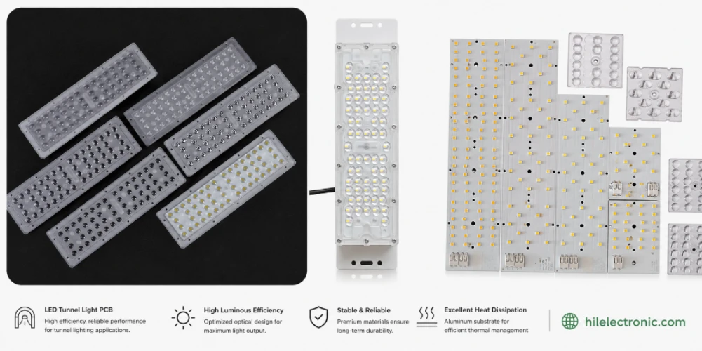
LED Tunnel Light PCB Manufacturing — High-Reliability Engines & Drivers
Figure 1. LED tunnel light PCB production and assembly...
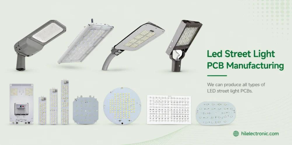
LED Street Light PCB Manufacturing & Assembly by Highleap Electronics
Figure 1. LED street light PCB production and assembly...
How to get a quote for PCBs
Let us run DFM/DFA analysis for you and get back to you with a report.
You can upload your files securely through our website.
We require the following information in order to give you a quote:
-
- Gerber, ODB++, or .pcb, spec.
- BOM list if you require assembly
- Quantity
- Turn time
In addition to PCB manufacturing, we offer a comprehensive range of electronic services, including PCB design, PCBA (Printed Circuit Board Assembly), and turnkey solutions. Whether you need help with prototyping, design verification, component sourcing, or mass production, we provide end-to-end support to ensure your project’s success. For PCBA services, please provide your BOM (Bill of Materials) and any specific assembly instructions. We also offer DFM/DFA analysis to optimize your designs for manufacturability and assembly, ensuring a smooth production process.