
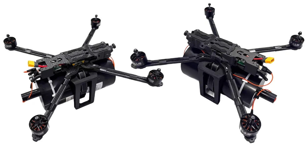
Anti Jamming Drone PCB Manufacturing and Assembly Services

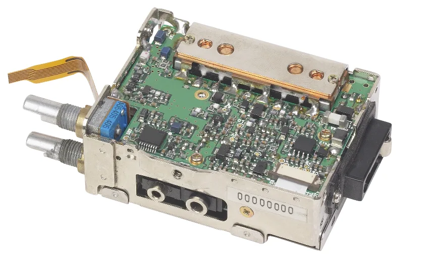
An anti jamming drone PCB is not a standard UAV control board with extra shielding. It is a purpose-built PCB architecture designed to maintain navigation, telemetry, video, and command performance under intentional jamming, co-site interference, and incidental electromagnetic noise from both onboard and external sources.
This matters across commercial, industrial, and defense UAVs. Near airports, broadcast towers, substations, or hostile RF environments, drone performance can degrade quickly if the PCB is not designed for interference resistance. A reliable anti jamming drone PCB depends on coordinated stack-up design, grounding, RF isolation, power integrity, component placement, and shielding from the start.
Quick answer
An anti jamming drone PCB maintains communication and navigation performance under electromagnetic interference through disciplined RF layout, continuous return-path design, controlled-impedance routing, GNSS front-end protection, EMI-aware power distribution, shielding, filtering, and fallback architectures such as inertial navigation or optical tethered data transmission in specialized systems. At board level, anti-jamming performance depends on how well sensitive receivers are isolated from noise, how clean the power rails remain under dynamic load, and how effectively the layout prevents interference from coupling into critical signal paths.
Table of Contents
- What an Anti Jamming Drone PCB Must Resist
- Core Layers of Board-Level Anti-Jamming Design
- Layer Stack and Grounding Architecture
- Shielding and RF Isolation Techniques
- Power Integrity Under High EMI Stress
- GNSS Hardening and Navigation Fallback
- Link Diversity and Fiber Optic Alternatives
- How to Test Anti-Jamming Performance
- Anti Jamming Drone PCB FAQ
What an Anti Jamming Drone PCB Must Resist
To design an anti jamming drone PCB correctly, it is important to define the interference mechanisms it must withstand. Not all “jamming” is deliberate. From a board-design perspective, the threat environment usually includes four categories:
- Intentional RF jamming: high-power interference directed at GNSS, telemetry, control links, or video links
- Incidental external EMI: strong nearby transmissions from radar, broadcast infrastructure, cellular systems, or industrial RF equipment
- Onboard self-interference: noise generated by ESCs, motors, switching regulators, high-speed processors, cameras, and radios sharing the same airframe
- Co-site interference: coupling between the drone’s own GNSS, telemetry, video, command, and payload RF systems
The board cannot solve every system-level problem by itself, but it strongly influences receiver sensitivity, link margin, phase noise, power cleanliness, and susceptibility to unwanted coupling. In practice, a weak PCB architecture can turn a theoretically capable anti-jamming design into an unreliable product.
Core Layers of Board-Level Anti-Jamming Design
Layer 1: Physical EMI hardening
The first layer of anti-jamming is physical robustness at the PCB level: continuous reference planes, controlled-impedance RF routing, shielding over sensitive receiver sections, short return-current loops, and layout separation between noisy and sensitive circuits. If the RF front end is desensitized, compressed, or contaminated by local noise, higher-level mitigation methods will have limited value.
Layer 2: Link resilience and frequency diversity
Frequency-hopping, spread-spectrum signaling, channel agility, and redundant links all depend on stable hardware implementation. The PCB must support low-noise synthesizer supplies, good isolation between transmit and receive paths, low-jitter clocking, and RF routing that preserves impedance and minimizes leakage. These same principles also apply to broader drone PCB design, but anti-jamming applications require tighter control of coupling paths, shielding boundaries, and power-domain cleanliness.
Layer 3: Navigation resilience
GNSS signals are inherently weak and therefore vulnerable to both jamming and interference. A professional anti jamming drone PCB supports multi-constellation GNSS, front-end filtering, clean antenna biasing, low-noise amplification, and tightly controlled placement around the receiver. It should also support navigation continuity through IMU integration and, where required, higher-level sensor fusion or advanced antenna systems such as CRPA on specialized platforms.
Layer Stack and Grounding Architecture
A typical anti-jamming UAV board uses 6 to 10 layers, although more complex platforms may require additional layers to isolate RF, GNSS, high-speed digital, and high-current power domains. The key principle is not to split ground indiscriminately, but to maintain continuous reference planes and predictable return paths while separating noisy and sensitive functions through placement, routing discipline, filtering, and localized power regulation.
For RF and GNSS traces, uninterrupted reference planes are critical. Any split, slot, or poorly stitched transition beneath a sensitive signal path can increase impedance discontinuity, radiation, and susceptibility. A robust anti jamming drone PCB therefore emphasizes stack-up symmetry, continuous ground reference, stitched shielding boundaries, and tightly managed via transitions.
| Layer | Typical function | Design objective |
|---|---|---|
| L1 (Top) | RF, GNSS front end, critical analog, shield cans | Shortest sensitive paths, controlled impedance, minimal exposure to noisy zones |
| L2 | Continuous ground plane | Primary low-inductance reference for L1 routing; no plane interruptions under RF or GNSS paths |
| L3 | High-speed digital or internal signals | Route processor, radio, memory, or camera interfaces with controlled return paths |
| L4 | Ground or quiet reference plane | Additional shielding and return-path stabilization for inner-layer routing |
| L5 | Power distribution | Separate noisy and sensitive supply regions with filtering and local regulation |
| L6 | Ground plane | Reference for analog and low-speed control layers |
| L7 | Sensors, control, low-speed interfaces | Keep IMU, barometer, serial buses, and housekeeping signals away from RF hot zones |
| L8 (Bottom) | Power, motor-related routing, connectors | Confine high current and switching activity to the least sensitive area of the stack |
In higher-end designs, the stack-up is often refined with impedance modeling and electromagnetic analysis rather than by rule of thumb alone. This becomes even more important in integrated drone solutions that combine telemetry, GNSS, video transmission, onboard compute, and payload electronics within the same compact platform.
Shielding and RF Isolation Techniques
Shield cans with stitched grounding boundaries
Shield cans remain one of the most effective board-level defenses for drone RF electronics. The shield perimeter should land on a continuous grounded pad ring with dense via stitching to one or more solid ground planes. The objective is to reduce electric-field leakage, suppress cavity coupling, and limit interference bypassing the shield wall through the substrate or sparse grounding points.
Compartmentalized RF zones
On complex RF boards, it is often beneficial to isolate the LNA, synthesizer or VCO, PA, transceiver, and sensitive baseband sections into separate shielded regions or carefully separated zones. This helps reduce local coupling, especially when transmit power and receiver sensitivity coexist in close physical proximity.
Controlled-impedance feed lines
Antenna feeds, GNSS traces, and inter-stage RF connections should be routed as controlled-impedance structures with continuous reference planes and carefully managed transitions. Grounded via fences or coplanar grounding features may be used where the RF geometry supports them. The goal is not simply adding more copper, but achieving predictable field containment and low-loss signal transport.
Connector and cable-entry protection
Even when the PCB itself is well designed, interference often enters through external cables, harnesses, and antenna connectors. Common board-level countermeasures include ESD protection, common-mode filtering where appropriate, chassis-to-board bonding strategy, and controlled connector placement relative to sensitive receiver circuits.
Power Integrity Under High EMI Stress
Power integrity is one of the most underestimated aspects of anti-jamming PCB design. A drone may appear to have a radio problem when the root cause is actually power rail contamination, converter harmonics, transient ground bounce, or supply droop during motor load changes.
In an anti jamming drone PCB, the power architecture must be designed to keep sensitive RF and GNSS blocks electrically quiet even while the airframe experiences dynamic current demand. That usually means:
- Separate power treatment for sensitive domains: GNSS, RF front end, clocks, and precision sensors should not share noisy supply paths with motors, high-power transmitters, or compute bursts
- Switching pre-regulation with local post-regulation: a practical architecture is to use efficient DC-DC conversion upstream and then apply LDO cleanup near the most noise-sensitive blocks
- Ferrite beads and filtering used intentionally: beads can help suppress high-frequency noise when correctly selected and placed, but they are not a substitute for sound return-path design
- Converter placement discipline: keep switching regulators, inductors, and hot current loops physically distant from GNSS antennas, LNAs, reference oscillators, and receiver inputs
- Low-impedance decoupling strategy: decoupling should be matched to the frequency content and current transients of each domain, not applied as a generic checklist
Where GNSS is involved, designers should also verify that switching frequencies, harmonics, spurious emissions, and clock products do not reduce receiver sensitivity in the relevant bands. A design that passes functional bring-up may still underperform in the field if internal emissions raise the effective noise floor near the navigation receiver. For high-reliability builds, these requirements should also be reflected in manufacturing execution and process consistency, especially when working with a qualified drone PCB manufacturer.
GNSS Hardening and Navigation Fallback
For many UAVs, the most vulnerable subsystem is not the main telemetry radio but the navigation receiver. GNSS signals arrive at very low power, making them susceptible to both intentional jamming and incidental interference. As a result, GNSS hardening deserves dedicated board-level attention in any serious anti jamming drone PCB.
Key design priorities include:
- Multi-constellation GNSS support: GPS, Galileo, GLONASS, and BeiDou improve availability and redundancy, although constellation diversity alone does not constitute full anti-jamming capability
- Front-end filtering and LNA protection: SAW or BAW filters, low-noise amplification, and clean active-antenna biasing help preserve receiver sensitivity
- Careful antenna feed routing: short, impedance-controlled, well-referenced feed lines reduce insertion loss and coupling risk
- Isolation from digital and power noise: keep GNSS away from switching regulators, processor clocks, camera lanes, and motor-current return paths
- Support for fallback navigation: a clean IMU interface and reliable sensor-fusion path improve continuity when GNSS performance degrades
For advanced or defense-grade platforms, CRPA (controlled reception pattern antenna) architectures can suppress interference spatially by shaping antenna response. Supporting CRPA at PCB level is significantly more demanding than routing a single GNSS feed because it requires phase consistency, tightly controlled channel matching, low-noise front-end design, and disciplined layout symmetry. Programs with elevated survivability requirements may also evaluate specialized military fiber drone PCB architectures where mission profile, communication resilience, and system integration demand a more hardened approach.
In practice, robust navigation resilience usually comes from a combination of good GNSS front-end design, inertial sensing, timing supervision, and flight-control logic that can degrade gracefully instead of failing abruptly when satellite signals become unreliable.
Link Diversity and Fiber Optic Alternatives
No single radio technique is sufficient for every interference environment. Many anti-jamming drone platforms improve resilience through link diversity: separate command and payload links, multiple frequency bands, adaptive channel management, directional antennas, and physical separation between radios sharing the same airframe.
At PCB level, this requires careful coexistence design. The board must reduce self-interference between transmitters and receivers, isolate clock and LO leakage, and prevent high-power RF stages from collapsing receiver dynamic range. In many UAVs, the practical anti-jamming limit is not the protocol alone, but insufficient co-site isolation and noisy hardware implementation.
For tethered systems, fiber optic drone PCB architectures provide an important alternative. Fiber does not rely on wireless RF propagation for that communication segment, which makes it inherently resistant to classic RF jamming along the tethered data path. However, the associated transceivers, power conversion, and interface electronics still require proper EMI-aware PCB design.
Where tether management is part of the platform architecture, the optical path also depends on stable spool-side electronics and cable-handling integration. That subsystem design is discussed separately in our fiber optic tether spool PCB overview.
How to Test Anti-Jamming Performance
An anti jamming drone PCB should be validated long before final chamber qualification. Early board-level and subsystem-level testing can identify susceptibility problems while layout changes are still practical.
Recommended validation methods include:
- Conducted susceptibility testing: evaluate how supply rails and external interfaces behave under injected noise or transient disturbance
- Radiated susceptibility screening: expose the board or subassembly to controlled RF fields while monitoring GNSS lock, telemetry quality, and processor stability
- Antenna-port interference injection: measure receiver degradation, desensitization, blocking response, and recovery behavior under controlled interference
- Power-noise characterization under load: observe ripple, transients, and switching artifacts with motors, payload, compute, and radios active simultaneously
- GNSS performance under full-system activity: monitor carrier-to-noise behavior, reacquisition performance, position stability, and sensitivity while all onboard subsystems operate
- Co-site interference testing: verify that onboard links do not significantly degrade one another when transmitting concurrently
- Pre-compliance EMC review: use near-field probes, current probes, and spectral measurements to locate dominant emitters and coupling paths before formal compliance testing
These evaluations do not replace full environmental or EMC qualification, but they can reveal a large portion of grounding, shielding, placement, and power-integrity issues at a much earlier stage of development. When a tethered system is involved, the ground-side optical interface should also be validated as part of the full communication chain, including the electronics described in the fiber optic canister PCB design.
Anti Jamming Drone PCB FAQ
Does every drone need an anti jamming drone PCB?
Not every drone needs defense-grade anti-jamming architecture, but nearly every professional UAV benefits from EMI-aware PCB design. The required level of hardening depends on mission criticality, RF environment, operating altitude, payload sensitivity, and acceptable risk.
Can anti-jamming capability be retrofitted onto an existing PCB?
Some improvements can be added later, including shielding, filtering, cable treatment, and power cleanup. However, the most important factors—stack-up, return-path continuity, placement, isolation distances, and RF partitioning—are usually determined at the initial layout stage. Retrofits can help, but they rarely match a PCB designed for interference resistance from the beginning.
What standards are relevant?
Applicable requirements depend on the program and market. EMC, environmental, vibration, and mission-specific standards may all apply. In military contexts, programs often reference standards such as MIL-STD-461 for electromagnetic compatibility and MIL-STD-810 for environmental robustness, but exact qualification requirements should always be confirmed at system and contract level.
Is multi-constellation GNSS enough to claim anti-jamming capability?
No. Multi-constellation support improves availability and resilience, but it does not by itself guarantee resistance to deliberate jamming. True anti-jamming performance usually depends on front-end filtering, shielding, clean power, receiver dynamic range, antenna strategy, and navigation fallback design.
How can PCB design improve anti-jamming performance in drone systems?
PCB design plays a critical role in improving anti-jamming performance in drone systems. RF-aware stack-up planning, controlled-impedance routing, effective shielding, and clean power architecture help reduce electromagnetic interference and protect sensitive GNSS and communication circuits from signal disruption.
Highleap supports the fabrication and assembly of anti jamming drone PCB projects for industrial, tethered, and defense-oriented UAV platforms, including controlled-impedance fabrication, shielded board construction, and high-reliability assembly. We also provide dedicated PCB fabrication and PCB assembly services to ensure consistent performance for RF-sensitive and mixed-signal drone electronics.

Recommended Posts

Low CTE FR-4 PCB Manufacturing for Through-Hole Reliability
Low CTE FR-4 PCB manufacturing is used when a circuit...
Halogen Free FR-4 PCB Manufacturing for Controlled Material Builds
Halogen free FR-4 PCB manufacturing is used when a product...

FR408HR PCB Material for High-Reliability Multilayer Boards
FR408HR PCB material is selected when a multilayer board...

Nelco N4000-13EP PCB Manufacturer for High-Reliability Multilayer Boards
Nelco N4000-13EP PCB manufacturing is used for...
How to get a quote for PCBs
Let us run DFM/DFA analysis for you and get back to you with a report.
You can upload your files securely through our website.
We require the following information in order to give you a quote:
-
- Gerber, ODB++, or .pcb, spec.
- BOM list if you require assembly
- Quantity
- Turn time