
RO3206 PCB Manufacturing
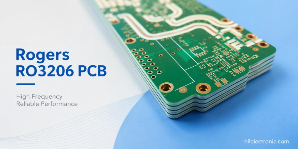
RO3206 PCB manufacturing is suited to miniaturized RF constructions where electrical spacing has to be reduced without losing control of the finished board. The manufacturing target is the simulated geometry after lamination and etch, not the nominal artwork dimensions. An RO3206 quotation should begin with the dimensions the product cannot exceed—not with a generic request for a “high-Dk Rogers board.” Rogers’ RO3200 series data sheet lists RO3206 with a process Dk of 6.15 ±0.15, a design Dk of 6.6 and a typical Df of 0.0027 at 10 GHz. Those values can shorten resonators and distributed networks, but the smaller geometry also gives line width, gap, dielectric thickness and finish variation more influence over the finished RF response. Where a higher-permittivity grade is considered, RO3210 high-Dk geometry and processing should be reviewed against the miniaturization target and manufacturing tolerance.
For Highleap Electronics, the practical task is to protect the customer’s approved geometry through material sourcing, imaging, etching, drilling, inspection and assembly. Prototype and volume routes are confirmed after the exact core thickness, copper, critical dimensions and acceptance method are reviewed. Published material data remain design references; the production release must use the approved construction and current supplier documentation. Highleap checks the compact RF layers for registration, copper definition, via placement and finished dielectric thickness. Where assembly is included, the RF keep-outs and component pads should remain consistent with the fabrication drawing so the PCBA does not introduce a second geometry change. Exact material property values should be checked against the current supplier documentation for the specified grade and construction.
The manufacturing focus for RO3206 is miniaturized RF geometry. The finished board should preserve the released conductor dimensions and dielectric spacing while maintaining registration and plated-hole quality through the complete fabrication sequence.
How Much Miniaturization Does the Project Actually Need?
Space pressure can come from an enclosure, antenna array pitch, module footprint, weight target or integration with other electronics. The design should state which dimension is constrained and how much reduction is required. If the product can tolerate a slightly larger layout, a lower-Dk material may offer wider conductors, broader bandwidth or easier tuning. If the outline is fixed, RO3206 can be a rational way to reduce electrical length.
| Decision factor | RO3206 may be attractive when | Reason to reconsider |
|---|---|---|
| Available area | The filter or resonator must fit a tightly defined module. | The enclosure still allows a larger, less sensitive structure. |
| Bandwidth | The topology can meet bandwidth after high-Dk loading. | Very broad bandwidth is more important than size. |
| Line and gap capability | Critical geometry remains within stable production limits. | Simulation requires features with little manufacturing margin. |
| Tuning strategy | Prototype correlation and controlled compensation are possible. | No first-article measurement or tuning loop is available. |
| Volume | Material utilisation and process controls can be justified. | A low-volume project cannot absorb special tooling or test cost. |
How much smaller will the circuit become?
The reduction depends on topology and electromagnetic field distribution; it cannot be promised from the material name alone. The engineer should compare complete layouts in the field solver, including conductor thickness, ground spacing, solder mask and enclosure. Highleap should receive the selected geometry, not an expectation that the factory redesign the RF circuit during quotation.
Is RO3206 suitable for broadband antennas?
Some antenna structures can use high-Dk materials, but high dielectric loading can reduce physical size while affecting bandwidth and radiation behaviour. The correct choice depends on antenna type, efficiency target, radome and ground structure. Highleap can manufacture the approved antenna and feed network; final radiated performance needs the assembled product and customer test method.
The tradeoffs are explained more broadly in miniaturized RF PCB design. Material choice is one lever among topology, lumped loading, multilayer integration and packaging.
The Hidden Cost of Higher Dielectric Constant
Miniaturization concentrates sensitivity. A small change in conductor width can represent a larger percentage of the intended geometry. A small change in dielectric thickness can move impedance and resonance. Narrow gaps challenge imaging and etching. Surface finish and copper profile can become a larger portion of the conductor. These effects do not make RO3206 unmanufacturable; they mean the design needs a realistic tolerance budget. A comparison with RT/duroid 6006 microwave builds should keep material properties, thickness and processing requirements separate.
Why can a smaller RF circuit be harder to manufacture?
A large resonator may tolerate a small absolute etch change with little frequency impact. A smaller resonator with narrower lines and gaps may not. The design team should sweep manufacturing variation in simulation. Highleap can provide expected fabrication ranges for the proposed thickness and copper, allowing the engineer to decide whether the nominal geometry has enough margin.
Dielectric thickness and copper condition
The exact laminate thickness and copper cladding should be frozen. If the circuit uses a hybrid stackup, the bond-line thickness and press result must also be included. Copper profile, treatment and final plating affect loss and geometry. The RFQ should not permit automatic substitution to another foil or thickness even when the material family is unchanged.
Projects with strict conductor-loss requirements should review high-Dk Rogers PCB fabrication and identify which copper and process assumptions were used in simulation.
Etch compensation is a controlled engineering action
CAM compensation can move the artwork so the finished trace or gap meets the target. It should not be applied blindly to resonators or coupled structures. Highleap asks the customer to classify critical dimensions and may return a compensation proposal for approval. Finished measurements from the first article can then be used to refine production data.
Surface finish and assembly lands
RF lines may be left with a selected finish while component pads require solderability and shelf life. The drawing should distinguish them. Thick or variable finish can change narrow conductors. Solder mask may load the field. The assembly layout should minimise stubs at component pads and transitions where the RF model is sensitive.
Material scope: the Rogers product name is used to identify the laminate specified for the PCB build. Highleap Electronics provides PCB fabrication and assembly, while the laminate is sourced and verified separately.
Correlating Simulation, Prototype and Production
A successful RO3206 product normally passes through a correlation loop. The designer supplies the electromagnetic model inputs and critical dimensions. The factory proposes a producible stackup and compensation. A first article is built and measured. The design or artwork is adjusted if needed. Only then is the production release frozen. Skipping this loop may save days at the quotation stage and lose weeks later.
Define the first-article question
The prototype should answer more than “does the board work?” It should determine whether the finished conductor dimensions match the model, whether material thickness is within the required range, whether the frequency response correlates, and whether the assembly introduces additional shift. Measurement can be performed on a coupon, a bare RF structure or the assembled module depending on the product.
Dimensional report and RF test
Highleap can provide agreed critical-dimension measurements and production records. RF testing must be defined by fixture, connector, calibration plane, frequency range and acceptance limit. A vague note such as “test RF performance” cannot be quoted consistently. The RF PCB testing plan should separate bare-board evidence from system-level radiated or functional tests.
Release compensation to volume production
After correlation, freeze the artwork revision, stackup, material lot rules, copper, surface finish and inspection points. If a later material or thickness change is proposed, reopen the electrical review. High-volume repeatability depends more on controlled change than on holding every physical dimension to an unnecessarily extreme tolerance.
What to Freeze Before Requesting an RO3206 PCB Quote
The RFQ should include exact RO3206 thickness and copper, critical RF dimensions, stackup if multilayer, finish and mask boundaries, drill and edge details, prototype and production quantities, and the required first-article evidence. If Highleap is also assembling the module, provide the BOM, centroid, assembly drawing, shield or housing interfaces and functional-test method.
- Material stock and special-order lead time are confirmed before a prototype date is promised.
- Prototype, low-volume and production pricing can be separated so tooling and test costs are visible.
- Payment method, currency and shipping route are confirmed with the quotation.
- International express is suitable for many prototypes; volume orders can use agreed freight.
- Lot records support post-delivery engineering review and corrective action.
Highleap can support fast high-frequency PCB manufacturing when the material and test route are available. “Fast” should mean a controlled schedule with known inputs, not an unconditional promise for any thickness or quantity.
Cost is driven by material utilisation, copper, thickness, layer count, tolerance, hybrid lamination, testing and order volume. See the practical Rogers PCB cost factors before comparing quotations that may include different constructions or inspection scopes.
Build a tolerance budget before asking for the tightest factory limit
The electrical model should show how frequency, impedance or coupling changes across expected line-width, gap and thickness ranges. That sensitivity can be translated into manufacturing tolerances. This is better than specifying the smallest number found on a capability chart, which may increase cost without improving product performance.
Highleap can review the proposed limits against copper, panel size and feature density. If one dimension is difficult, the design may be adjusted to reduce sensitivity. The objective is stable production, not a one-time prototype at the edge of capability.
Use prototype variants to shorten correlation
When approved by the RF designer, a first panel can include controlled variants in resonator length or coupling gap. All variants use the same material and process, making it easier to separate design sensitivity from lot variation. The selected production geometry is then frozen after measurement.
Assembly process can move the response
Solder volume, component tolerance, placement, shields and connectors can change a miniaturized circuit. The assembly drawing should identify orientation and mechanical interfaces. If Highleap assembles the module, stencil and placement review are coordinated with the RF layout. A bare-board response should not be used as the only acceptance criterion when the assembled product is highly sensitive.
Packaging should protect precision surfaces
RF boards can be damaged by abrasion, contamination or bent panels during transport. Highleap selects separators, trays, antistatic packaging and moisture protection according to finish and assembly state. The quotation can state whether units ship individually, in arrays or as assembled modules.
Production price should improve after qualification
The prototype may include engineering, material minimums, dimensional reports and RF coupons. Volume production can spread tooling and use a stable panel. Highleap can provide separate prototype and recurring prices so buyers do not mistake qualification cost for the long-term unit price.
Power and thermal limits may override the smallest geometry
A compact RF circuit can carry higher current density and concentrate heat. Conductor width, copper thickness, ground connection and housing thermal path should be checked before shrinking the layout. The best RO3206 design is not always the smallest possible design; it is the smallest construction that meets loss, temperature and reliability requirements.
If a power amplifier or high-current component is present, Highleap reviews thermal vias, copper areas, metal interfaces and assembly. The customer should provide power dissipation and allowable temperature so the board design is not judged only by frequency response.
Connector and fixture launches should be designed with the coupon
A precise circuit can be measured incorrectly through a poor launch. Test connectors, probes and calibration structures should be included in the measurement plan. Highleap can fabricate the launch geometry and fixture board, but the RF engineer should define the calibration plane and de-embedding method.
Use sampling that protects the critical response
First articles can receive full dimensional inspection. Volume lots may use sampling for critical lines and gaps, with material identity and electrical test controlled on every lot. If process capability changes, the sampling plan can be tightened. This is more efficient than measuring every non-critical feature on every board.
Supplier substitution should be prohibited unless requalified
RO3206 thickness, foil and construction belong to the electrical design. A different high-Dk laminate is not an automatic equivalent. Highleap can propose alternatives when supply requires it, but the customer should approve revised modelling and prototype evidence before use.
Quality and after-sales communication
Highleap’s quality response begins with the approved drawing and observed failure. Dimensional, material, assembly and test records are compared with the customer’s sample. If the issue is confirmed, containment and corrective action are communicated. If the board meets specification, the data help the customer investigate components, fixtures or enclosure effects.
Convenient delivery for prototypes and production
Prototype boards and assembled RF modules can be packed in trays or separated layers to protect critical surfaces. International express is normally practical for samples; scheduled production can use agreed air freight or courier. Payment, tax documentation and shipping responsibility are stated in the quotation so the technical team is not delayed by commercial ambiguity.
RF design review should identify tuning features
Some modules include trim areas, optional components or alternate resonator lengths. These should be documented rather than left as unexplained copper. Highleap can preserve designated tuning structures and ensure they are not removed during CAM cleanup. If the customer expects laser or mechanical tuning after fabrication, the process and inspection need to be included in the project plan.
Component sourcing can influence the final frequency response
Capacitor tolerance, package parasitics, connector type and shield dimensions can shift a compact circuit. When Highleap sources components, approved manufacturer part numbers and substitution rules should be supplied. Commercially convenient alternatives are not automatically electrically equivalent at RF.
BOM availability is reviewed together with laminate stock. This allows the customer to see whether PCB or components control the delivery date and prevents a completed bare board from waiting for a long-lead RF device.
Repeatability should be reviewed across fabrication and assembly
Production yield is a combined result. Critical line dimensions can be stable while solder volume or component placement varies, or the reverse. Highleap can correlate board lot, assembly lot and functional test when turnkey service is used. This combined traceability is useful for professional buyers who need a supplier to support both PCB and PCBA issues.
International orders need an agreed communication route
Technical questions, approval files, payment and shipment should use a revision-controlled communication path. Highleap confirms the sales and engineering contacts for the order. Tracking details and packing lists are supplied at shipment, while technical changes require written approval. This reduces the risk created by informal messages across time zones.
What should appear on the purchase order?
Reference the approved material, thickness, copper, fabrication drawing, stackup and artwork revision. State the required first-article or production records and whether substitutions need written approval. Include the assembly revision and approved component list if Highleap supplies PCBA. This small amount of purchasing discipline prevents a repeat order from being treated as a generic RO3206 board.
Material note: confirm the latest Rogers controlled data, exact RO3206 construction and copper in the design model and purchase specification. For quotation, state the grade, finished thickness, copper, RF band, smallest features and assembly scope. This gives the engineering review enough detail to determine the appropriate process route.

Recommended Posts

Taconic RF 35 vs RO4350B PCB
Table of contentsRF-35 vs RO4350B Procurement and...

TMM4 Filter PCB Manufacturing
TMM4 filter PCB manufacturing is controlled by the...

TMM3 PCB Manufacturing for RF Modules
TMM3 PCB manufacturing is most useful where the RF module...

TMM6 PCB Fabrication
TMM6 fabrication is the process-control page for a mid-Dk...
How to get a quote for PCBs
Let’s run DFM/DFA analysis for you and get back to you with a report. You can upload your files securely through our website. We require the following information in order to give you a quote:
-
- Gerber, ODB++, or .pcb, spec.
- BOM list if you require assembly
- Quantity
- Turn time
For PCBA services, please provide your BOM (Bill of Materials) and any specific assembly instructions. We also offer DFM/DFA analysis to optimize your designs for manufacturability and assembly, ensuring a smooth production process.