
NP-175F PCB Laminate for High-Reliability Multilayer Boards
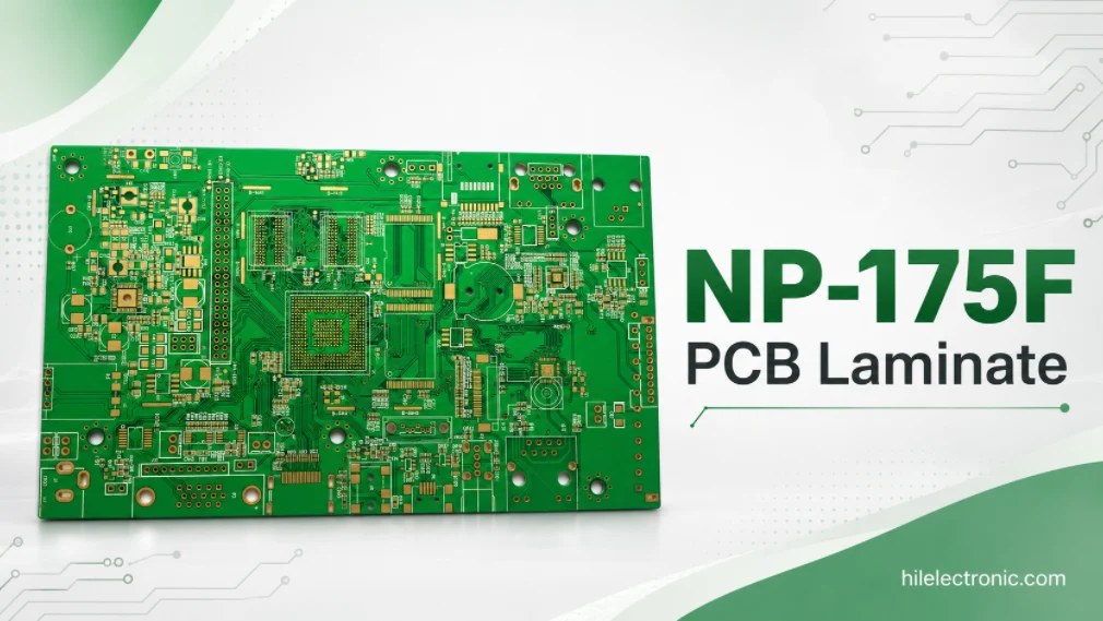
NP-175F PCB laminate is a Nan Ya high-Tg, filled multifunctional epoxy laminate and prepreg system used when a multilayer PCB project requires stronger thermal reliability, CAF resistance, and lead-free assembly compatibility than ordinary FR-4. In PCB manufacturing, the material name affects laminate sourcing, prepreg selection, stackup control, lamination, drilling, plating, impedance calculation, soldering, documentation, and repeat production stability. When manufacturing and assembling NP-175F boards, laminate identification and the approved thermal process should remain consistent from bare-board production through reflow.
Highleap Electronics manufactures and assembles PCB and PCBA products using customer-approved laminate systems such as Nan Ya NP-175F. Highleap does not produce copper-clad laminate, prepreg, resin, or glass fabric. When NP-175F is specified by a fabrication drawing, AVL, customer specification, or qualification record, the production task is to source the approved construction, confirm the stackup, control the process route, and deliver a finished PCB or assembled PCBA that matches the project requirement.
Related manufacturing topics: NP-175F projects often connect with multilayer PCB manufacturing, prepreg material for multilayer PCB, PCB impedance control, PCB assembly services, and broader 10-layer PCB materials planning.
NP-175F PCB Laminate Manufacturing for High-Reliability Multilayer Boards
NP-175F is commonly selected when a PCB design requires a high-Tg FR-4 class laminate with better thermal resistance than ordinary FR-4. For purchasing and engineering teams, the key issue is whether the specified NP-175F construction matches the board thickness, copper weight, layer count, prepreg combination, impedance requirement, assembly process, and production volume.
In multilayer production, the material callout belongs in the fabrication package. The drawing defines the approved laminate or equivalent approval rules. The stackup identifies the core, prepreg, resin content, copper thickness, finished board thickness, and impedance requirement. If the project is already qualified with NP-175F, substitution to another high-Tg FR-4 requires customer approval before purchasing or tooling.
Production intent behind an NP-175F material callout
A callout such as “Nan Ya NP-175F” usually appears when thermal reliability, plated-through-hole robustness, CAF resistance, or lead-free reflow stability matters. These requirements are common in industrial controls, communication boards, power electronics, automotive-related electronics, and high-layer-count PCB assemblies.
- High-Tg multilayer PCB manufacturing
- Lead-free compatible PCB and PCBA projects
- Boards requiring improved thermal stress resistance
- Designs with dense vias or plated-through-hole reliability concerns
- Customer-approved material systems requiring controlled sourcing
For adjacent material planning, engineering teams often compare NP-175F with ITEQ IT-180A, Kingboard KB-6160, Kingboard KB-6165, and other high-Tg FR-4 materials. The final selection follows the customer drawing, AVL, qualification status, and production risk review.
NP-175F Material Properties and Datasheet Values for PCB Design
NP-175F is not a generic FR-4 substitute. Its most relevant production properties include Tg, Td, Z-axis CTE, CAF resistance, dielectric constant, dissipation factor, moisture absorption, peel strength, flammability, and compliance status. These values help determine whether the material fits the stackup, reflow profile, reliability target, and controlled impedance requirement.
Published values are useful for engineering review, but they remain tied to the specific data sheet revision, test condition, glass style, resin content, and construction. Dk and Df vary with frequency and laminate or prepreg construction. Final production values must be confirmed against the current supplier data sheet, certificate, and approved stackup.
| Property | Typical / datasheet reference | Manufacturing relevance |
|---|---|---|
| Material supplier | Nan Ya Plastics / Nan Ya electronic materials family | Identifies the approved laminate source for purchasing, AVL control, and traceability |
| Material type | High-Tg filled multifunctional epoxy laminate and prepreg | Used as a controlled FR-4 class material for reliable multilayer PCB production |
| Tg | 170°C class; typical 173°C by DSC / TMA in available data | Supports lead-free reflow and high-temperature multilayer reliability better than ordinary Tg FR-4 |
| Glass transition test method | DSC / TMA values appear in available datasheet data | Prevents confusion when comparing Tg values from different supplier data sheets |
| Td | Typical 351°C; specification commonly listed as 340°C minimum for 5% weight loss | Important for lead-free thermal exposure, lamination, and assembly heat cycles |
| Z-axis CTE | 40–60 ppm/°C before Tg; 250–270 ppm/°C above Tg in available data | Affects plated-through-hole reliability and thermal cycling performance |
| Thermal conductivity | Typical 0.49 W/mK in available data | Useful for baseline thermal review, but not a replacement for copper, vias, and mechanical heat paths |
| Dk | Approximately 4.1–4.5 in available data, depending on frequency and construction | Used for impedance modeling and stackup confirmation |
| Df | Approximately 0.011–0.019 in available data, depending on frequency and construction | Suitable for many industrial and digital boards, but not an ultra-low-loss high-speed laminate |
| CAF resistance | Datasheet indicates pass / AABUS depending on test condition | Important for dense spacing, via reliability, humid environments, and high-reliability multilayer boards |
| Moisture absorption | Typical data appears around 0.10–0.30% depending on condition and construction | Influences storage, baking, soldering risk, and reliability in humid service environments |
| Peel strength | Depends on copper foil type, copper thickness, and post-process condition | Supports copper adhesion review for fabrication, rework, and thermal stress exposure |
| Flammability and compliance | UL94 V-0; RoHS compliant in available datasheet note | Supports common commercial compliance requirements, subject to the purchased grade and documentation needs |
Material data must match the purchased construction
Datasheet values provide the engineering baseline. The finished board still depends on the core and prepreg construction purchased for the project. Glass style, resin content, copper foil type, board thickness, and lamination structure affect dielectric height, impedance, dimensional stability, and mechanical behavior. For controlled builds, the fabrication package specifies the approved NP-175F construction instead of relying only on a material family name.
NP-175F PCB Laminate Standards and Certifications
Standards and certifications help connect the laminate data sheet to real PCB procurement and documentation. They do not replace engineering review, but they give buyers and engineers a common language for material approval, drawing notes, compliance files, and repeat production records.
NP-175F data should be checked against the current Nan Ya document, UL record, customer AVL, and any project-specific compliance requirements. When a drawing asks for certificates or traceability, those items need to be discussed before quotation rather than after the boards are finished.
Applicable standards and compliance items
| Item | How it appears in NP-175F projects | Why it matters to procurement and production |
|---|---|---|
| IPC-4101 | Available NP-175F data lists IPC-4101 slash sheets including /21, /24, /26, /97, /98, /99, /101, and /126 | Helps define laminate/prepreg classification and approved material requirements |
| IPC-TM-650 | Many laminate properties are reported with IPC-TM-650 test method references | Allows engineering teams to understand how values such as Tg, Td, CTE, peel strength, and moisture absorption are measured |
| UL94 V-0 | Listed in available NP-175F data | Supports flammability requirements for commercial and industrial electronics |
| UL recognition | Verify the current UL file, material type, thickness range, and recognition status before controlled production | Prevents documentation gaps when customers require UL-supported material records |
| RoHS | Available NP-175F data states RoHS compliance | Supports common regulatory documentation for electronics manufacturing |
| REACH | Confirm with current supplier declaration when required by the customer | Important for EU-facing products and compliance documentation packages |
| Halogen-free status | NP-175F should not be assumed to be halogen-free; available data identifies bromine flame retardant use | Avoids incorrect compliance claims when the project requires halogen-free FR-4 |
For customers that require material certificates, RoHS declarations, REACH statements, UL details, or lot traceability, the RFQ package needs to identify those documentation requirements at the beginning. This keeps compliance work aligned with material purchasing and production planning.
NP-175F PCB Stackup and Prepreg Control
NP-175F PCB stackup planning is critical when the board has controlled impedance, high layer count, dense vias, thick copper, or lead-free PCBA requirements. A stackup that looks acceptable in a design tool may still need manufacturing adjustment if the selected prepreg style, resin content, copper distribution, and final thickness cannot be held consistently in production.
For multilayer builds, the stackup defines the NP-175F core and prepreg structure clearly. If the board includes impedance-controlled traces, the design package also identifies target impedance, tolerance, trace width, trace spacing, reference plane layer, and whether impedance coupons or reports are required. This is especially important for boards routed with Ethernet, DDR, LVDS, USB, PCIe, clock lines, or mixed-signal interfaces.
Prepreg selection affects thickness, resin flow, and impedance
NP-175F prepreg selection is not left open when finished dielectric thickness is important. Resin flow, remaining copper percentage, glass style, and lamination conditions affect final dielectric thickness. If the design has tight impedance tolerance, the PCB impedance control review takes place before CAM tooling, not after the board is already released.
- Core and prepreg thickness by layer
- Finished copper thickness after plating
- Reference planes for controlled impedance
- Glass style and resin content where required
- Impedance coupon and report requirements
- Press cycle and lamination notes for repeat production
For high-layer-count projects, related planning may also include prepreg material for multilayer PCB and 10-layer PCB materials. These pages support broader stackup decisions when NP-175F is part of a larger material or reliability discussion.
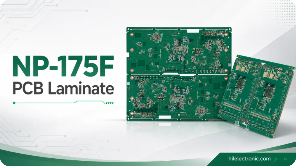
NP-175F vs Standard FR-4 and Other High-Tg FR-4 Materials
NP-175F should not be treated as a generic replacement for every FR-4 board. It is a high-Tg filled epoxy material used when the design needs stronger thermal and reliability performance than ordinary FR-4. At the same time, it is not an ultra-low-loss material for the most demanding high-speed backplane or RF designs. The right comparison depends on the customer requirement, approved material list, thermal budget, signal performance, cost target, and production availability.
| Material option | Typical Tg class | Typical project intent | Engineering and manufacturing decision |
|---|---|---|---|
| Standard FR-4 | Typical mid-Tg or standard Tg, depending on supplier | Cost-effective general PCB manufacturing | Suitable when layer count, reflow exposure, and reliability requirements are moderate |
| NP-175F PCB laminate | 170°C class | High-Tg, filled FR-4 class multilayer PCB with improved thermal and CAF performance | Use when the drawing, AVL, or reliability target requires NP-175F or an approved equivalent |
| Other high-Tg FR-4 materials | Often 170–180°C class, depending on grade | Alternative high-reliability multilayer builds | Review only if customer-approved; examples include selected ITEQ, Kingboard, Shengyi, EMC, Isola, Panasonic, or Nan Ya materials |
| Low-loss or ultra-low-loss laminates | Varies by material family | High-speed digital or RF designs with tighter insertion loss requirements | Consider when signal loss, long trace length, or data rate exceeds what NP-175F is intended to support |
Approved equivalents require engineering confirmation
Substituting NP-175F with another high-Tg FR-4 material may be possible in some projects, but it is not a silent purchasing decision. Resin system, Tg, Td, CTE, Dk, Df, CAF performance, UL recognition, prepreg availability, stackup behavior, and qualification history can all affect the finished PCB. If the customer drawing specifies NP-175F, any equivalent material requires engineering approval before purchasing or tooling.
When cost pressure or material availability becomes part of the discussion, the decision moves through a controlled engineering change process. Related background can be linked through FR-4 PCB cost increase when the project team needs to understand how material selection affects quotation and lead time.
Typical Applications of NP-175F PCB Laminate
NP-175F fits projects where standard FR-4 is not enough for thermal reliability, lead-free assembly, or dense multilayer construction, while ultra-low-loss high-speed laminates are not required. The material choice is especially relevant when the product must move from prototype to repeat production without changing the approved material system.
Application fit still depends on layer count, copper weight, impedance, temperature exposure, operating voltage, assembly process, and customer qualification rules. The list below describes common use cases rather than automatic approval for every design.
Common PCB and PCBA applications
- Industrial controllers and automation boards
- Telecommunication equipment and networking hardware
- Server support boards and high-layer-count digital electronics
- Automotive ECUs and automotive-related control modules
- Power supplies, chargers, and power management electronics
- Battery systems and energy storage control boards
- Medical electronics requiring stable multilayer PCB production
- Test instruments and embedded control systems
NP-175F PCB Fabrication for CAF and Thermal Reliability
NP-175F is often selected for boards where plated-through-hole reliability, CAF resistance, and thermal cycling performance are important. These advantages only become useful when the board design and fabrication process are aligned. Via size, aspect ratio, drill quality, desmear, plating thickness, copper balance, lamination control, and cleanliness all contribute to the final reliability result.
For dense multilayer boards, CAF risk is not solved by material selection alone. Spacing, glass style, resin coverage, drill smear control, ionic cleanliness, humidity exposure, operating voltage, and customer test requirements all matter. A practical NP-175F fabrication review connects material choice with layout rules, process capability, and inspection criteria.
Fabrication controls that protect high-reliability builds
- Drilling quality and hole-wall preparation
- Desmear and plated-through-hole copper thickness
- Inner-layer registration and lamination alignment
- Copper balance to reduce bow, twist, and stress
- Minimum spacing review for CAF-sensitive areas
- Thermal stress inspection and reliability documentation when required
For boards using NP-175F in a high-layer-count structure, multilayer PCB manufacturing capability becomes part of the material decision. A laminate with strong thermal properties still requires stable drilling, plating, lamination, solder mask, surface finish, and final inspection to produce a reliable PCB.
NP-175F PCB Assembly for Lead-Free PCBA Production
NP-175F PCB assembly is planned together with the bare board process when the project will be delivered as a finished PCBA. Lead-free reflow, selective soldering, wave soldering, press-fit connectors, high-mass components, and multiple thermal cycles can all stress the laminate and plated-through holes. The assembly process is therefore considered before the fabrication stackup is frozen.
For turnkey PCBA, the material requirement connects to BOM sourcing, stencil design, surface finish, reflow profile, inspection plan, and final test requirements. If the board has BGAs, QFNs, power devices, large connectors, or high copper weight, the assembly review may affect solder mask design, via-in-pad treatment, thermal relief, and panelization.
PCBA review items for NP-175F boards
- Lead-free reflow compatibility and thermal profile review
- Surface finish selection such as ENIG, immersion silver, OSP, or lead-free HASL
- Stencil aperture planning for dense SMT components
- AOI, X-ray, ICT, or functional test requirements
- Connector and through-hole soldering process control
- BOM risk, component lifecycle, and packaging requirements
When fabrication and assembly are purchased together, PCB assembly services should be reviewed at the same time as the NP-175F stackup. This reduces the risk of discovering assembly conflicts after the bare PCB has already been manufactured.
NP-175F PCB Quote and Documentation Requirements
An accurate NP-175F PCB laminate quote requires more than a material name. The supplier must understand the board construction, production volume, reliability requirements, and whether the order is for bare PCB manufacturing or complete PCBA delivery. Incomplete data can lead to wrong assumptions about laminate availability, prepreg selection, impedance, inspection, and assembly cost.
The quotation package identifies the approved material requirement clearly. If the customer allows equivalents, the approval rule needs to be stated. If the project must remain NP-175F because of qualification, the drawing and purchase notes make that restriction clear. This is especially important for repeat production, regulated products, and customer-qualified electronics.
RFQ files that help avoid material and production delays
- Gerber, ODB++, or IPC-2581 manufacturing data
- Fabrication drawing with NP-175F material callout
- Stackup with core, prepreg, copper, and finished thickness
- Controlled impedance table and tolerance requirements
- Surface finish, solder mask, silkscreen, and marking requirements
- Annual volume, prototype quantity, and production forecast
- BOM, pick-and-place file, and assembly drawing for PCBA orders
- Required reports, certificates, traceability, or customer documentation
For a controlled production review, submit the data through the Highleap quick quote form. Engineering feedback before production helps confirm material availability, stackup feasibility, impedance targets, assembly constraints, documentation requirements, and long-term production consistency.
NP-175F PCB Laminate FAQ
The following questions cover common procurement, engineering, and manufacturing concerns when NP-175F appears on a PCB fabrication drawing or material specification.
What is NP-175F PCB laminate?
NP-175F is a Nan Ya high-Tg filled multifunctional epoxy laminate and prepreg system used for high-reliability FR-4 class multilayer PCB manufacturing. It is commonly considered when the project requires stronger thermal reliability, lead-free assembly compatibility, and CAF resistance than ordinary FR-4.
Is Highleap a producer of NP-175F laminate?
No. Highleap Electronics is a PCB manufacturing and PCB assembly factory. The company does not produce NP-175F laminate or prepreg. For PCB projects, the factory sources customer-approved laminate materials and uses them to manufacture bare boards or assembled PCBAs according to the drawing and production requirements.
Is NP-175F the same as standard FR-4?
No. NP-175F belongs to the FR-4 class, but it is a high-Tg filled material intended for more demanding multilayer and lead-free assembly applications. Standard FR-4 may be suitable for lower-cost general electronics, while NP-175F is usually selected for stronger thermal and reliability requirements.
Can NP-175F replace another high-Tg FR-4 material?
It can only replace another material if the customer approves the substitution. Tg alone is not enough to confirm equivalence. Dk, Df, CTE, Td, CAF performance, UL recognition, prepreg availability, stackup behavior, and qualification history also need to be checked.
Is NP-175F suitable for impedance-controlled PCB designs?
Yes, NP-175F can be used in many impedance-controlled multilayer PCB designs. The stackup must define dielectric thickness, copper weight, trace geometry, reference planes, and the required impedance tolerance. For very high-speed or long-channel designs, lower-loss materials may need to be evaluated separately.
Does NP-175F support sequential lamination?
NP-175F can be considered for sequential lamination projects when the selected construction, press cycle, copper distribution, via structure, and reliability requirements are compatible with the fabricator’s process. Sequential lamination should be reviewed case by case because repeated thermal cycles can affect dimensional stability, resin flow, plated-hole reliability, and final board cost.
Is NP-175F suitable for HDI PCB?
NP-175F may be used in some HDI or dense multilayer PCB projects, but HDI suitability depends on dielectric thickness, prepreg availability, laser drilling requirements, microvia reliability, lamination sequence, and customer qualification rules. For advanced HDI designs, the stackup and via structure should be reviewed before layout release.
Is NP-175F a halogen-free laminate?
NP-175F should not be assumed to be halogen-free. Available datasheet information identifies a bromine flame retardant mechanism while also listing RoHS compliance and UL94 V-0 flammability. If halogen-free compliance is required, the drawing or AVL should specify a suitable approved halogen-free laminate instead of relying on NP-175F by name.
How should I specify NP-175F on a PCB fabrication drawing?
Specify the approved laminate model, laminate supplier, core and prepreg construction, stackup, finished board thickness, copper weight, impedance requirements, surface finish, IPC or customer specifications, documentation requirements, and whether equivalent materials are allowed. If equivalents are allowed, the approval conditions should be stated clearly.
What files are needed for an NP-175F PCB quote?
Send Gerber or ODB++ files, fabrication drawing, stackup, impedance table, quantity, lead time target, and assembly files if PCBA is required. For repeat production or customer-qualified products, include material restrictions, certificates, inspection requirements, and traceability expectations.
Request an NP-175F PCB Laminate Engineering Review
NP-175F PCB laminate projects should begin with a clear material callout, controlled stackup, and complete manufacturing package. Highleap Electronics can review the fabrication files, stackup, impedance requirements, assembly data, and documentation needs before production so that the material requirement is correctly translated into a reliable PCB or PCBA build.
Prepare your Gerber or ODB++ data, fabrication drawing, stackup, BOM, pick-and-place file, and expected quantity, then submit the package through the Highleap quick quote form. Engineering review before production helps confirm material availability, stackup feasibility, impedance targets, long-term production consistency, and avoid material substitutions, qualification delays, and unnecessary redesigns.

Recommended Posts

Taconic RF 35 vs RO4350B PCB
Table of contentsRF-35 vs RO4350B Procurement and...

TMM4 Filter PCB Manufacturing
TMM4 filter PCB manufacturing is controlled by the...

TMM3 PCB Manufacturing for RF Modules
TMM3 PCB manufacturing is most useful where the RF module...

TMM6 PCB Fabrication
TMM6 fabrication is the process-control page for a mid-Dk...
How to get a quote for PCBs
Let’s run DFM/DFA analysis for you and get back to you with a report. You can upload your files securely through our website. We require the following information in order to give you a quote:
-
- Gerber, ODB++, or .pcb, spec.
- BOM list if you require assembly
- Quantity
- Turn time
For PCBA services, please provide your BOM (Bill of Materials) and any specific assembly instructions. We also offer DFM/DFA analysis to optimize your designs for manufacturability and assembly, ensuring a smooth production process.