
High Speed PCB Material Selection for Signal Integrity
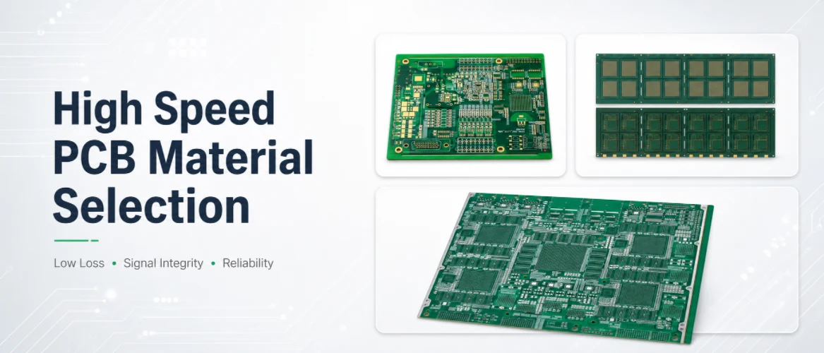
Figure 1. High speed PCB material selection.
On a high-speed board, the laminate is part of the circuit. The dielectric’s electrical properties shape every transmission line on the board, set the propagation delay, and determine how much of each edge survives the trip from driver to receiver. Choosing the material is therefore one of the highest-leverage decisions in the entire design — and in 2026 it is also one of the most supply-constrained. This guide walks through the material properties that matter for signal integrity, when standard FR-4 stops being adequate, what AI and networking hardware actually require, and how to lock the choice in early so the program is not derailed by an unavailable grade.
Material Properties That Matter
Four laminate properties dominate high-speed material selection. The dielectric constant (Dk) sets the impedance and propagation velocity. The dissipation factor (Df) sets the dielectric loss. The glass transition temperature (Tg) sets the thermal robustness of the resin during assembly and operation. And the coefficient of thermal expansion (CTE), particularly in the z-axis, governs reliability through thermal cycling. For high-speed signal integrity specifically, Dk and Df are the leading pair: Dk because impedance control depends on it, Df because insertion loss depends on it.
A fifth, often-overlooked property is Dk stability — how constant the dielectric constant stays across frequency and across the glass-weave pattern. Glass-weave effects can cause local Dk variation that produces skew between differential pairs, which is why high-rate designs sometimes specify spread-glass or mechanically rotated layouts. The relationships among these parameters are detailed in dielectric constant and loss tangent and the broader high-speed PCB materials overview.
Understanding Dk, Df, Tg, and CTE
Dk (dielectric constant) determines how fast a signal propagates and what trace geometry yields a target impedance. A lower, more stable Dk supports faster propagation and easier impedance control; a Dk error directly produces an impedance error, so the design must use the real laminate Dk rather than a datasheet nominal.
Df (dissipation factor, loss tangent) determines how much signal energy the dielectric absorbs. Standard FR-4 has a Df acceptable at low speed but too high for long high-rate channels; low-loss grades use specialized resins to drop Df by an order of magnitude or more, which is what keeps insertion loss within budget at high SerDes rates.
Tg (glass transition temperature) is the temperature at which the resin softens. High-Tg material (170+) resists the thermal stress of lead-free assembly and high-temperature operation; but specifying high-Tg where the thermal profile does not require it adds roughly 20–40% material cost without benefit, an avoidable expense in the current market. See high-Tg PCB material for detail.
CTE (coefficient of thermal expansion), especially the z-axis value, governs how much the board expands through thermal cycling. A high z-axis CTE stresses plated through-holes and is a reliability concern for high-layer-count and thermally cycled boards. Low-CTE materials and balanced stack-ups mitigate this.
When FR4 Is No Longer Suitable
FR-4 remains the right material for the great majority of boards, but it stops being suitable when the channel’s loss budget can no longer tolerate FR-4’s Df over the required trace length at the required data rate. As a practical guide, FR-4 becomes marginal as channels move into the higher gigabit ranges and lengths grow; at 112G and 224G SerDes rates, low-loss material becomes mandatory because FR-4’s insertion loss would close the eye. RF and microwave front ends, where Df and Dk stability are paramount, also fall outside FR-4’s envelope.
The key discipline is to make this judgment per channel and per layer, not per board. Many designs mix a handful of high-rate channels with a majority of ordinary signals, and the high-rate requirement applies only to specific layers. This is what makes hybrid stack-ups so valuable: the premium material goes only where the loss budget demands it. The threshold analysis is in what is high-speed PCB and the design guidance in high-speed PCB design.
Material Choices for AI and Networking Hardware
AI and high-speed networking hardware sit at the top of the material ladder. The progression of AI compute platforms has driven a climb up the CCL grade scale, and each step changes resin chemistry, copper-foil profile, and glass-cloth grade simultaneously — multiplying material cost rather than adding to it. Industry figures place M6 at roughly 3–5× standard FR-4, M7 at 6–9×, M8 at 10–15×, and M9 Q-glass at 15–20×, with a next-generation M10 grade in qualification targeting Df below 0.002 for 448G+ signaling.
For most high-speed networking boards, mid-loss to low-loss grades (M4–M7 class) cover the requirement, with families such as Panasonic Megtron 6/7, Isola I-Tera/I-Speed, TUC Tachyon, EMC, and Iteq grades commonly used. The highest-rate AI compute boards and midplanes move into M8/M9 territory with HVLP copper foil and quartz glass cloth. Because these grades are the most constrained materials in the current PCB material shortage, the selection must pair the electrical choice with a qualified equivalent and an allocation plan. The application detail is in AI server PCB materials and the supply context in the AI server PCB demand analysis.
Stack-Up Planning Considerations
Stack-up planning is where material selection becomes a buildable board. Several considerations matter for high-speed designs. Every high-rate signal layer needs a solid adjacent reference plane to provide a clean return path; a signal layer referenced to a split or gapped plane develops impedance discontinuities and EMI. The dielectric thicknesses between signal and reference layers set the impedance together with the trace width, so they must be chosen as a system using the real laminate Dk. Symmetry matters for warpage control, especially on high-layer-count boards. And in 2026, the stack-up should be planned for availability as well as performance: confining the scarcest grade to the layers that need it, and qualifying an equivalent grade, builds a structural hedge against allocation loss.
A hybrid stack-up using a premium grade on critical layers and high-Tg FR-4 on the rest can reduce premium-material consumption substantially while still meeting loss and impedance targets — and it limits an allocation crisis to a few layers rather than the whole board. The mechanics are in our high-speed PCB stack-up guide and the PCB stack-up guide.
Manufacturer Review Before Fabrication
A manufacturer review before fabrication is the step that turns a material selection into a confirmed, buildable, sourceable design. For a high-speed board the review confirms the impedance using the actual laminate Dk, checks reference-plane continuity under high-rate signals, validates that the specified grade matches the loss budget without over-specification, and — uniquely important in the current market — checks the availability of the specified grade and identifies a qualified equivalent. Catching a material or impedance problem at this stage costs a review cycle; catching it after fabrication costs a respin and a lost material allocation.
Highleap Electronics provides confirmed stack-up calculations using measured laminate Dk values and a pre-fabrication review that covers impedance, reference-plane integrity, and material availability for high-speed designs.
Get a High-Speed PCB Stack-Up Review
Highleap Electronics fabricates high-speed boards across mid-loss and low-loss grades through our high-speed PCB manufacturing and high frequency PCB programs.
High Speed PCB Material FAQs
Which material properties matter most for high-speed signal integrity->
Dielectric constant (Dk) and dissipation factor (Df) lead, because they set impedance and dielectric loss. Tg matters for thermal robustness and CTE for thermal-cycling reliability. Dk stability across frequency and glass weave also affects skew on differential pairs.
At what data rate does FR-4 stop being suitable->
It depends on channel length, but FR-4 becomes marginal as channels move into higher gigabit rates and longer lengths, and low-loss material becomes mandatory at 112G/224G SerDes rates because FR-4’s insertion loss would close the eye. The judgment should be made per channel and per layer.
What is the CCL grade ladder and why does it matter for cost->
Each step up the grade ladder (FR-4 to M4, M6, M7, M8, M9) changes resin, foil, and glass simultaneously, multiplying material cost. Approximate multipliers versus FR-4: M6 ~3-5x, M7 ~6-9x, M8 ~10-15x, M9 ~15-20x. Specifying higher than needed is expensive.
Should I use a hybrid stack-up->
Often yes, when only some layers carry high-rate signals. Putting premium material only on critical layers and FR-4 on the rest reduces premium-material consumption and cost while still meeting loss and impedance targets, and it limits supply risk to a few layers.
Why must impedance be calculated with the real laminate Dk->
Because a Dk error translates directly into an impedance error. Using a datasheet nominal instead of the actual process Dk can put the board’s impedance outside tolerance, degrading the signal integrity the high-speed material was chosen to protect.

Recommended Posts

Taconic RF-35 PCB Manufacturing Service — Prototype Through Volume Production
Figure 1. Taconic RF-35 PCBTaconic RF-35 is the workhorse...

Isola Astra MT77 PCB Manufacturing
Figure 1. Isola Astra MT77 PCB ManufacturingIsola Astra...

Custom Rogers RO4835 PCB Fabrication & Assembly Services
Figure 1. Rogers RO4835 PCBRogers RO4835 PCB is a...

Nelco N4000-13 PCB Material and Manufacturing Guide | Highleap Electronics
Figure 1. Nelco N4000-13 PCBNelco N4000-13 PCB is a...
How to get a quote for PCBs
Let’s run DFM/DFA analysis for you and get back to you with a report. You can upload your files securely through our website. We require the following information in order to give you a quote:
-
- Gerber, ODB++, or .pcb, spec.
- BOM list if you require assembly
- Quantity
- Turn time
For PCBA services, please provide your BOM (Bill of Materials) and any specific assembly instructions. We also offer DFM/DFA analysis to optimize your designs for manufacturability and assembly, ensuring a smooth production process.